QP50-6-SD2 Pacific Silicon Sensor, QP50-6-SD2 Datasheet - Page 2
QP50-6-SD2
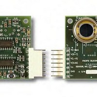
Manufacturer Part Number
QP50-6-SD2
Description
Photodiodes 50mm2 quadrant detector module
Manufacturer
Pacific Silicon Sensor
Type
Quadrant Moduler
Datasheet
1.QP50-6-SD2.pdf
(2 pages)
Specifications of QP50-6-SD2
Photodiode Material
Silicon
Maximum Operating Temperature
+ 70 C
Minimum Operating Temperature
0 C
Mounting Style
Through Hole
Product
Photodiode
Lead Free Status / RoHS Status
Lead free / RoHS Compliant
Other names
10-025


The QP50-6SD2 outputs are labeled as B-T for bottom minus top, L-
R for left minus right. The output voltages are obtained by routing the
diode element currents into current-to-voltage amplifiers with a gain
of 10
V
V
V
I
x and y. Looking down through the window of the photodiode, the
quadrants are identified in drawing on page one.
Beam Size
The light spot applied to the QP50-6SD2 must be smaller than the diameter of the quadrant photodiode array. The detector active area has a
diameter of 7.8 millimeters. If the light spot is too large, it may be reduced to fit the photodiode array by use of a lens. A decrease in output
signal strength is observed as the light spot crosses the separation boundary of the quadrants, usually referred to as the “gap”. This effect is
more pronounced as the diameter of the light spot decreases, as a larger percentage of the light spot’s power falls within the non-active gap.
For this reason, the minimum light beam diameter should be a least one millimeter. A lens may be used to increase the beam diameter.
Photodiode Bias Operation
The QP50-6SD2 array may be operated either in the zero bias or the reverse bias mode. Pin 1 is connected, via a resistor divider, to the non-
inverting input of a voltage follower operational amplifier. This line may be left unterminated, grounded or connected to a voltage source of
zero volts to operate in the zero bias mode. If the photodiode bias line is connected to a positive voltage source (but less than Vcc), then the
photodiode elements in the array will be biased at 0.91 x VBias. Do not connect Pin 1 to negative voltages, as this will forward bias the
photodiode array, making it inoperable and possibly damaging the circuit.
Use of Sum and Difference Signals for Alignment
The sum output signal may be used to help preliminary alignment of the QP50-6SD2 to the source light beam. First, the beam or the QP50-
6SD2 is adjusted for maximum sum output signal. Second, the beam or QP50-6SD2 is adjusted until the L-R and B-T signals are at minimum.
This procedure results in the beam being centered on the quad photodiode array.
Signal Null Detector for Servo Applications
A common application for the QP50-6SD2 is a signal null detector as part of a servo system that maintains the position of a light beam. Errors
in beam position are reported by the QP50-6SD2 and may be used to adjust a positioning device that restores the beam or the beam’s source
to a null position.
Speed of Response
Increasing the photodiode bias voltage will increase the speed of the QP50-6SD2. Operating with zero reverse bias is sufficient for many
applications (-3dB is around 150 kHz at 880 nm). As noted above, Pin 1 is provided for applying positive bias voltage to the quad for higher
frequency response. Care should be taken not to exceed the circuit common mode values and the breakdown voltage of the quad photodiode.
See Absolute Maximum Ratings on page one for maximum values.
Temperature Considerations
The operation temperature must be between 0 to 70 °C. For best resolution the temperature should be kept at or below 25 °C. Thermal
gradients across the detector will cause position errors and should be avoided.
Offsets
Precision components are used in the circuitry but as much as 10 millivolts of dark offset may still be present in the outputs. If this causes a
problem the offsets should be removed externally.
USA:
Pacific Silicon Sensor, Inc.
5700 Corsa Avenue, #105
Westlake Village, CA 91362 USA
Phone (818) 706-3400
Fax (818) 889-7053
Email:
www.pacific-sensor.com
9/24/2010
X,Y
B-T
L-R
SUM
= [(I
= [(I
is the sum of the currents generated by photodiode elements
4
= [(I
:
sales@pacific-sensor.com
3,4
2,3
1,2,3,4
) - (I
) - (I
) • (10
1,2
1,4
)] • (10
)] • (10
4
) on Pad 4.
4
4
) on Pad 2.
) on Pad 3.
Proud Members of the Silicon Sensor International AG Group of companies
APPLICATION NOTES
QP50-6-TO8
BLOCK DIAGRAM
i2
i3
i1
i4
V2 = i2 X 10
V3 = i3 X 10
V1 = i1 X 10
V4 = i4 X 10
X0.91
4
4
4
4
International sales:
Silicon Sensor International AG
Peter-Behrens-Str. 15
D-12459 Berlin, Germany
Phone +49 (0)30-63 99 23 10
Fax +49 (0)30-63 99 23 33
Email:
www.silicon-sensor.de
SUM AND
DIFFERENCE
AMPLIFIERS
sales@silicon-sensor.de
X1
-
+
+15V
-15V
PHOTODIODE BIAS
PAD 1
(V3 +V4) - (V1 + V2)
PAD 2
(V2 +V3) - (V1 + V4)
PAD 3
V1 + V2 + V3 + V4
PAD 4
PAGE 2 OF 2
GROUND PAD 6
-15V PAD 7
+15V PAD 5
Related parts for QP50-6-SD2
Image
Part Number
Description
Manufacturer
Datasheet
Request
R

Part Number:
Description:
Photodiodes Quadrant 7.98 Area w/0.018mm Gap
Manufacturer:
Pacific Silicon Sensor
Datasheet:

Part Number:
Description:
Photodiodes Quadrant 4 X 11.78mm 7.8mm Active Area
Manufacturer:
Pacific Silicon Sensor
Datasheet:

Part Number:
Description:
Photodiodes Quadrant 7.8mm Dia Area with 18Um Gaps
Manufacturer:
Pacific Silicon Sensor
Datasheet:

Part Number:
Description:
Photodiodes Quadrant 7.8mm Dia Area with 42um Gaps
Manufacturer:
Pacific Silicon Sensor
Datasheet:
Part Number:
Description:
Photodiodes 50mm2 quadrant detector module
Manufacturer:
Pacific Silicon Sensor
Datasheet:

Part Number:
Description:
Photodiodes 50mm2 quadrant detector module
Manufacturer:
Pacific Silicon Sensor
Datasheet:
Part Number:
Description:
Photodiodes Quadrant 1.19x1.19mm Area w/0.018mm Gap
Manufacturer:
Pacific Silicon Sensor
Datasheet:

Part Number:
Description:
Photodiodes Quadrant 7.8mm Dia Area with 18Um Gaps
Manufacturer:
Pacific Silicon Sensor
Datasheet:

Part Number:
Description:
Photodiodes Wavelength Selective Sensor 2.75mm2 Area
Manufacturer:
Pacific Silicon Sensor
Datasheet:

Part Number:
Description:
Photodiodes High Speed Si APD 100um Active Area
Manufacturer:
Pacific Silicon Sensor
Datasheet:

Part Number:
Description:
Photodiodes High Speed Si APD 800um Active Area
Manufacturer:
Pacific Silicon Sensor
Datasheet:

Part Number:
Description:
Photodiodes High Speed Si APD 230um Active Area
Manufacturer:
Pacific Silicon Sensor
Datasheet:

Part Number:
Description:
Photodiodes High Speed Si APD 500um Active Area
Manufacturer:
Pacific Silicon Sensor
Datasheet:

Part Number:
Description:
Photodiodes UV/Blue enhanced 5.5x6.1mm Area
Manufacturer:
Pacific Silicon Sensor
Datasheet:

Part Number:
Description:
Photodiodes UV/Blue enhanced 3.57mm Dia Area
Manufacturer:
Pacific Silicon Sensor
Datasheet: