ILQ615-1 Vishay, ILQ615-1 Datasheet - Page 3
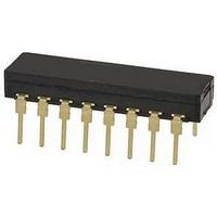
ILQ615-1
Manufacturer Part Number
ILQ615-1
Description
Transistor Output Optocouplers Phototransistor Out Quad CTR 40-80%
Manufacturer
Vishay
Specifications of ILQ615-1
Isolation Voltage
5300 Vrms
Forward Current
60 mA
Maximum Input Diode Current
60 mA
Maximum Reverse Diode Voltage
6 V
Output Device
Transistor
Output Type
DC
Configuration
4
Input Type
DC
Maximum Collector Emitter Voltage
70 V
Current Transfer Ratio
80 %
Maximum Forward Diode Voltage
1.3 V
Minimum Forward Diode Voltage
1 V
Maximum Collector Current
50 mA
Maximum Power Dissipation
500 mW
Maximum Operating Temperature
+ 100 C
Minimum Operating Temperature
- 55 C
Package / Case
PDIP-16
No. Of Channels
4
Optocoupler Output Type
Phototransistor
Input Current
10mA
Output Voltage
70V
Opto Case Style
DIP
No. Of Pins
16
Lead Free Status / RoHS Status
Lead free / RoHS Compliant
Lead Free Status / RoHS Status
Lead free / RoHS Compliant, Lead free / RoHS Compliant
Available stocks
Company
Part Number
Manufacturer
Quantity
Price

Part Number:
ILQ615-1
Manufacturer:
SIEMENS/西门子
Quantity:
20 000


Notes
• Stresses in excess of the absolute maximum ratings can cause permanent damage to the device. Functional operation of the device is not
(1)
Note
• Minimum and maximum values are tested requierements. Typical values are characteristics of the device and are the result of engineering
Document Number: 83652
Rev. 1.6, 04-Mar-11
ABSOLUTE MAXIMUM RATINGS (T
PARAMETER
COUPLER
Storage temperature
Operating temperature
Junction temperature
Soldering temperature
Package power dissipation ILD615
Derate linearly from 25 °C
Package power dissipation ILQ615
Derate linearly from 25 °C
Isolation test voltage
Isolation voltage
Total power dissipation
Creepage distance
Clearance distance
Isolation resistance
ELECTRICAL CHARACTERISTCS (T
PARAMETER
INPUT
Forward voltage
Breakdown voltage
Reverse current
Capacitance
Thermal resistance, junction to lead
OUTPUT
Collector emitter capacitance
Collector emitter leakage current, -1, -2
Collector emitter leakage current, -3, -4
Collector emitter breakdown voltage
Emitter collector breakdown voltage
Thermal resistance, junction to lead
PACKAGE TRANSFER CHARACTERISTICS
Channel/channel CTR match
COUPLER
Capacitance (input to output)
Insulation resistance
Channel to channel isolation
implied at these or any other conditions in excess of those given in the operational sections of this document. Exposure to absolute
maximum ratings for extended periods of the time can adversely affect reliability.
Refer to reflow profile for soldering conditions for surface mounted devices (SMD). Refer to wave profile for soldering conditions for through
hole devices (DIP).
evaluations. Typical values are for information only and are not part of the testing requirements.
(1)
For technical questions, contact:
Optocoupler, Phototransistor Output
2 mm distance from case bottom
V
amb
V
amb
IO
V
IO
I
V
IO
F
V
V
= 500 V, T
TEST CONDITION
TEST CONDITION
(Dual, Quad Channel)
= 500 V, T
CE
IO
R
= 10 mA, V
= 500 V, T
= 25 °C, unless otherwise specified)
= 25 °C, unless otherwise specified)
= 0 V, f = 1 MHz
I
= 0 V, f = 1 MHz
= 5 V, f = 1 MHz
CE
I
I
V
V
I
E
F
R
V
CE
CE
= 0.1 mA
= 10 mA
t = 1 s
= 0.5 mA
= 10 μA
R
= 6 V
= 10 V
= 10 V
amb
amb
A
CE
= 25 °C
= 100 °C
= 25 °C
= 5 V
optocoupleranswers@vishay.com
CTRX/CTRY
SYMBOL
BV
BV
R
R
SYMBOL
I
I
C
V
C
C
CEO
CEO
THJL
THJL
R
V
I
V
BR
R
CE
CEO
ECO
T
IO
V
F
O
S
T
T
P
R
R
IORM
amb
T
ISO
stg
sld
tot
IO
IO
j
Vishay Semiconductors
1 to 1
MIN.
10
500
70
1
6
7
12
- 55 to + 150
- 55 to + 100
VALUE
ILD615, ILQ615
10
10
5300
5.33
6.67
100
260
400
500
890
250
7
7
TYP.
1.15
0.01
10
750
500
6.8
0.8
30
25
12
11
2
5
14
MAX.
2 to 1
100
1.3
10
50
www.vishay.com
mW/°C
mW/°C
UNIT
V
mW
mW
mW
mm
mm
°C
°C
°C
°C
RMS
V
P
UNIT
VAC
K/W
K/W
μA
nA
nA
pF
pF
pF
V
V
V
V
3
Related parts for ILQ615-1
Image
Part Number
Description
Manufacturer
Datasheet
Request
R

Part Number:
Description:
Transistor Output Optocouplers Phototransistor Out Quad CTR 160-320%
Manufacturer:
Vishay
Datasheet:
Part Number:
Description:
Transistor Output Optocouplers Phototransistor Out Quad CTR 100-200%
Manufacturer:
Vishay
Datasheet:
Part Number:
Description:
Transistor Output Optocouplers Phototransistor Out Quad CTR 63-125%
Manufacturer:
Vishay
Datasheet:

Part Number:
Description:
Transistor Output Optocouplers Phototransistor Out Quad CTR > 100-200%
Manufacturer:
Vishay
Part Number:
Description:
Optocoupler
Manufacturer:
Vishay
Datasheet:
Part Number:
Description:
Optocoupler
Manufacturer:
Vishay
Datasheet:
Part Number:
Description:
Optocoupler
Manufacturer:
Vishay
Datasheet:
Part Number:
Description:
Transistor Output Optocouplers Phototransistor Out Quad CTR > 63-125%
Manufacturer:
Vishay
Part Number:
Description:
Transistor Output Optocouplers Phototransistor Out Quad CTR > 100-200%
Manufacturer:
Vishay
Part Number:
Description:
Transistor Output Optocouplers Phototransistor Out Quad CTR > 160-320%
Manufacturer:
Vishay
Part Number:
Description:
Transistor Output Optocouplers Phototransistor Out Quad CTR > 100-200%
Manufacturer:
Vishay
Part Number:
Description:
Transistor Output Optocouplers Phototransistor Out Quad CTR > 100-200%
Manufacturer:
Vishay

Part Number:
Description:
Transistor Output Optocouplers Phototransistor Out Quad CTR > 160-320%
Manufacturer:
Vishay
Datasheet:
Part Number:
Description:
Transistor Output Optocouplers Phototransistor Out Quad CTR > 100-200%
Manufacturer:
Vishay
Part Number:
Description:
Transistor Output Optocouplers Phototransistor Out Quad CTR > 40-80%
Manufacturer:
Vishay