VO3526 Vishay, VO3526 Datasheet

Triac & SCR Output Optocouplers 1.0A Load Current Power Phototriac

VO3526

Manufacturer Part Number
VO3526
Description
Triac & SCR Output Optocouplers 1.0A Load Current Power Phototriac
Manufacturer
Vishay
Datasheet

Specifications of VO3526

Isolation Voltage
5300 V
Package / Case
DIP-10
Configuration
1 Channel
Maximum Continuous Output Current
1 A
Maximum Input Current
50 mA
Maximum Operating Temperature
+ 85 C
Maximum Power Dissipation
1.2 W
Maximum Reverse Diode Voltage
5 V
Minimum Operating Temperature
- 40 C
Mounting Style
SMD/SMT
Zero-crossing Circuit
No
Output Device
PhotoTriac
Peak Output Voltage (vdrm)
600 V
Maximum Input Voltage
1.4 V
Maximum Output Voltage
600 V
No. Of Channels
1
Optocoupler Output Type
Phototriac
Input Current
10mA
Output Voltage
1.7V
Opto Case Style
DIP
No. Of Pins
10
Output Type
Phototriac
Rohs Compliant
Yes
Lead Free Status / RoHS Status
Lead free / RoHS Compliant
Lead Free Status / RoHS Status
Lead free / RoHS Compliant, Lead free / RoHS Compliant
DESCRIPTION
The VO3526 is an optically couple phototriac driving a power
triac in a DIP-10 (16) package. It provides a 5300 V of input
to output isolation.
Note
For additional information on the possible lead bend and VDE options refer to option information.
Notes
(1)
(2)
(3)
Document Number: 81842
Rev. 1.2, 23-Oct-08
ORDER INFORMATION
PART
VO3526
ABSOLUTE MAXIMUM RATINGS
PARAMETER
INPUT
LED continuous forward current
LED reverse voltage
OUTPUT
Repetitive peak off-state voltage
On-state RMS current
Peak nonrepetitive surge current
(50 Hz, peak)
COUPLER
Total power dissipation
Ambient temperature range
Storage temperature range
Soldering temperature
Isolation test voltage
T
Stresses in excess of the absolute maximum ratings can cause permanent damage to the device. Functional operation of the device is not
implied at these or any other conditions in excess of those given in the operational sections of this document. Exposure to absolute maximum
ratings for extended periods of the time can adversely affect reliability.
Refer to wave profile for soldering conditions for through hole devices.
Total power dissipation value is based on 2S2P PCB. Refer to power phototriac application note for PCB design tips.
amb
21081
= 25 °C, unless otherwise specified.
2
3
4
5
6
7
9, 13
11
15
Pin
LED anode
LED cathode
N/C
N/C
N/C
N/C
Triac T2
Triac T1
Triac gate
Function
(2)
2
3
4
5
6
7
For technical questions, contact: optocoupler.answers@vishay.com
Sine wave, 50 to 60 Hz,
TEST CONDITION
(1)
t ≤ 10 s max.
Power Phototriac
gate open
for 1.0 s
15
13
11
9
FEATURES
• Maximum trigger current (I
• Isolation test voltage 5300 V
• Peak off-state voltage 600 V
• Load current 1 A
• dV/dt of 500 V/µs
• Pure tin leads
APPLICATIONS
• Triac driver
• Programable controllers
• AC-output module
AGENCY APPROVALS
• UL - E52744 system code H
• CUL - E52744 system code H
• VDE - DIN EN 60747-5-5 (VDE 0884)
SYMBOL
I
V
T(RMS)
P
T
V
I
T
T
V
TSM
DRM
I
amb
diss
ISO
stg
sld
F
R
Tubes, DIP-10 (16)
REMARKS
Vishay Semiconductors
- 40 to + 125
- 40 to + 85
VALUE
5300
600
260
FT
5.0
1.0
1.2
50
10
RMS
): 10 mA
VO3526
www.vishay.com
UNIT
V
mA
°C
°C
°C
W
RMS
V
V
A
A
1

Related parts for VO3526

VO3526 Summary of contents

Page 1

... Triac T1 15 Triac gate 7 21081 DESCRIPTION The VO3526 is an optically couple phototriac driving a power triac in a DIP-10 (16) package. It provides a 5300 V of input to output isolation. ORDER INFORMATION PART VO3526 Note For additional information on the possible lead bend and VDE options refer to option information. ...

Page 2

... VO3526 Vishay Semiconductors ABSOLUTE MAXIMUM RATING CURVES Ambient Temperature (°C) 21296 A Fig Power Dissipation vs. Temperature THERMAL CHARACTERISTICS PARAMETER SYMBOL VALUE Maximum LED T jmax. junction temperature Maximum NOT T jmax. junction temperature Thermal resistance, θ NOT-B junction NOT to bord Thermal resistance, θ NOT-C ...

Page 3

... IN RMS dV/dt ( (fig RMS dV/dt (c) Fig dV/dt Test Circuit TEST CONDITION Input With snubber (0.022 µF, 47 Ω) Output = 40 °C On 4-layer PCB °C/ ° VO3526 Vishay Semiconductors MIN. TYP. MAX 0.9 1.4 1.7 100 25 210 0 TEST TEST dV/dt SYMBOL MIN. MAX. I ...

Page 4

... VO3526 Vishay Semiconductors SAFETY AND INSULATION RATINGS PARAMETER Climatic classification Pollution degree Tracking resistance (comparative tracking index) Highest allowable overvoltage Maximum working insulation voltage Insulation resistance at 25 °C Insulation resistance Insulation resistance at 100 °C Partial discharge test voltage Safety limiting values - ...

Page 5

... Fig Normalized Holding Current vs. Temperature Vishay Semiconductors 21303 t (µs) ON Fig Trigger Input Current vs. Turn-on Time 3 2.5 2 1 21304 Temperature (ºC) 6.0 5.5 5.0 4.5 4.0 3 21305 Pulse Width (µs) Fig Trigger Current vs. Trigger Pulse Width VO3526 100 80 100 www.vishay.com 5 ...

Page 6

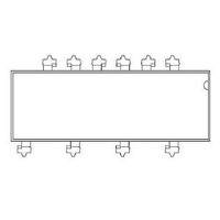
... VO3526 Vishay Semiconductors 3 2.8 2.6 2.4 2.2 2 1.8 1.6 1.4 1 100 200 300 400 21306 V (V) load Fig Trigger Current vs. V PACKAGE DIMENSIONS in inches (millimeters 0.779 (19.77) 0.790 (20.07) 0.030 (0.76) 0.045 (1.14) 4° 0.018 (0.46) 0.022 (0.56) 0.100 (2.54) typ. ...

Page 7

... Vishay Semiconductor GmbH, P.O.B. 3535, D-74025 Heilbronn, Germany Document Number: 81842 For technical questions, contact: optocoupler.answers@vishay.com Rev. 1.2, 23-Oct-08 Power Phototriac and may do so without further notice. VO3526 Vishay Semiconductors www.vishay.com 7 ...

Page 8

... Vishay product could result in personal injury or death. Customers using or selling Vishay products not expressly indicated for use in such applications their own risk and agree to fully indemnify and hold Vishay and its distributors harmless from and against any and all claims, liabilities, expenses and damages arising or resulting in connection with such use or sale, including attorneys fees, even if such claim alleges that Vishay or its distributor was negligent regarding the design or manufacture of the part ...

Related keywords