NCP5010EVB ON Semiconductor, NCP5010EVB Datasheet - Page 6
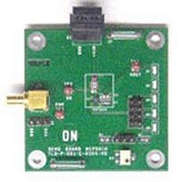
NCP5010EVB
Manufacturer Part Number
NCP5010EVB
Description
Power Management Modules & Development Tools EVAL BRD FOR NCP5010FCT1G
Manufacturer
ON Semiconductor
Datasheet
1.NCP5010EVB.pdf
(11 pages)
Specifications of NCP5010EVB
For Use With/related Products
NCP5010
Lead Free Status / RoHS Status
Lead free / RoHS Compliant


Demo Board NCP5010BIASEVB (DC/DC Boost
Converter)
provide a constant voltage. Here the network divider R2/R4
is used to sampling the output voltage and provide feedback
voltage to the FB input.
one of them like R2 = 10 kW, the value of R4 is given by:
Figure 12 is the schematic of the NCP5010 configured to
The Equation 2 is used to determine the value of V
For example, should one need a V
V OUT + V FB
R4 + R2
VPOWER
J4
J1
1
2
3
1
2
V
Figure 9. Schematic Diagram for Demo Board NCP5010BIASEVB
V OUT * V FB
CC
V FB
R2 ) R4
R2
OUT
TP4
CTRL
of 15 V. If we fix
NCP5010
A2
A3
CTRL
NC
NCP5010EVB/D
http://onsemi.com
(eq. 2)
(eq. 3)
OUT
V
.
CC
VOUT
1
2
L1
22 mH
6
U1
above−calculated value.
the converter is started by a high logic signal on the CTRL
pin a small current source (10 mA nominal) charges the
output capacitor (C2) up to 66 % of V
DC/DC boost converter enters the switching mode. Care
must be observed to ensure that the load does not sink more
than 2 mA during this phase until the output reaches
0.66 V
C1
C1
4.7 mF 6.3 V
Then choose a standard value that is close to the
R2 should be 2.2 to 22 kW and R4 lower than 1 MW.
The NCP5010 has built in short circuit protection so when
C2
4.7 mF
25 V
IN
(nom) to allow proper startup of the converter.
R4 + 10 3
V
TP2
OUT
R4
TBDk
R2
10k
15 * 0.5
J3
0.5
1
2
R1
100k
R3
500k
V
+ 287 kW
J2
OUT
IN
at which point the
(eq. 4)
Related parts for NCP5010EVB
Image
Part Number
Description
Manufacturer
Datasheet
Request
R

Part Number:
Description:
Boost Converter
Manufacturer:
ON Semiconductor
Datasheet:
Part Number:
Description:
ON Semiconductor [VOLTAGE REGULATOR]
Manufacturer:
ON Semiconductor
Datasheet:
Part Number:
Description:
357-036-542-201 CARDEDGE 36POS DL .156 BLK LOPRO
Manufacturer:
ON Semiconductor
Datasheet:
Part Number:
Description:
357-036-542-201 CARDEDGE 36POS DL .156 BLK LOPRO
Manufacturer:
ON Semiconductor
Datasheet:
Part Number:
Description:
357-036-542-201 CARDEDGE 36POS DL .156 BLK LOPRO
Manufacturer:
ON Semiconductor
Datasheet:
Part Number:
Description:
357-036-542-201 CARDEDGE 36POS DL .156 BLK LOPRO
Manufacturer:
ON Semiconductor
Datasheet:
Part Number:
Description:
357-036-542-201 CARDEDGE 36POS DL .156 BLK LOPRO
Manufacturer:
ON Semiconductor
Datasheet:
Part Number:
Description:
357-036-542-201 CARDEDGE 36POS DL .156 BLK LOPRO
Manufacturer:
ON Semiconductor
Datasheet:
Part Number:
Description:
357-036-542-201 CARDEDGE 36POS DL .156 BLK LOPRO
Manufacturer:
ON Semiconductor
Datasheet:
Part Number:
Description:
357-036-542-201 CARDEDGE 36POS DL .156 BLK LOPRO
Manufacturer:
ON Semiconductor
Datasheet:
Part Number:
Description:
357-036-542-201 CARDEDGE 36POS DL .156 BLK LOPRO
Manufacturer:
ON Semiconductor
Datasheet:
Part Number:
Description:
357-036-542-201 CARDEDGE 36POS DL .156 BLK LOPRO
Manufacturer:
ON Semiconductor
Datasheet:
Part Number:
Description:
Manufacturer:
ON Semiconductor
Datasheet:
Part Number:
Description:
Manufacturer:
ON Semiconductor
Datasheet: