AP561-PCB2500 TriQuint, AP561-PCB2500 Datasheet
AP561-PCB2500
Specifications of AP561-PCB2500
Available stocks


Related parts for AP561-PCB2500


AP561-PCB2500 Summary of contents
Page 1
... Vcc +5 +12 = 30dBm. AVG Rating +33 dBm Ordering Information Part No. AP561-F -55 to +150 ºC AP561-PCB900 158 ºC AP561-PCB2140 8.4 ° AP561-PCB2500 Standard T/R size = 500 pieces on a 7” reel. Functional Diagram Function Pin No. RF 4,5 9,10,11 OUT I 14 REF V 1 BIAS NC 2,3,7,8,12,13 ...
Page 2
... Microstrip line details: width = .043”, spacing = .050” r Evaluation Board Bias Procedure Following bias procedure is recommended to ensure proper functionality of AP561 in a laboratory environment. The sequencing is not required in the final system application. Turn-on Sequence: 1. Attach input and output loads onto the evaluation board. ...
Page 3
... S22 S(2,2) Swp Max Swp Max AP561 6GHz 6GHz Swp Min Swp Min 0.05GHz 0.05GHz S12 (ang) S22 (dB) S22 (ang) 29.12 -1.38 -106.01 8.71 -1.82 -138.64 1.08 -2.02 -164 ...
Page 4
... The edge of C20 is placed 380mil from the edge of C27. (12.9 9. The edge placed at 115mil from edge of AP561. (3.9 10. The edge of C28 is placed 230mil from the edge of R5. (7.8 11. The edge placed 180mil from the edge of C28. (6.1 12. 0 Ω jumpers can be replaced with copper trace in target application. ...
Page 5
... The edge of C27 is placed 43 mil from the edge of L1. (1.6 8. The edge of C20 is placed 380mil from the edge of C27. (14.6 9. The edge placed at 105mil from edge of AP561. (4 10. The edge of C28 is placed 200mil from the edge of R5. (7.7 11. 0 Ω jumpers can be replaced with copper trace in target application. Return Loss T=25° ...
Page 6
... Do not exceed 13V on Vcc or damage to D2 will occur. 4. Components shown on the silkscreen but not on the schematic are not used. 5. The edge of C34 is placed at 95mil from edge of AP561. (8.1 6. The edge of C33 is placed 375mil from the edge of C34. (32 7. The edge of C20 is placed 65mil from the edge of C33. (5.6 8 ...
Page 7
... The edge of C31 is placed at 35mil from edge of AP561. (3.1 6. The edge of L1 next to the edge of C31. 7. The edge of C34 is placed at 195mil from edge of AP561. (17.1 8. The edge of C33 is placed next to the edge of C34. 0 Ω jumpers can be replaced with copper trace in target application. ...
Page 8
... The edge of C32 is placed 40mil from the edge of C34. (3.7 7. The edge of C33 is placed 375mil from the edge of C32. (35 8. The edge of C30 is placed at 100mil from AP561 RFin pin. (9.3 9. The edge of C31 is placed 295mil from the edge of C30. (25.6 10. 0 Ω jumpers can be replaced with copper trace in target application. ...
Page 9
... The edge of C26 is placed next to the edge of C25. 7. The edge of C27 is placed 75mil from the edge of C26. (7.7 8. The edge of C24 is placed at 40mil from AP561 RFin pin. (4.1 9. The edge of C23 is placed next to the edge of C24. 10. 0 Ω jumpers can be replaced with copper trace in target application. ...
Page 10
... AP561 0.7-2.9 GHz 8W Power Amplifier 2.5-2.7 GHz Application Circuit (AP561-PCB2500) Typical O-FDMA Performance at 25°C Frequency (GHz) 2.5 2.6 2.7 Channel Power +30 +30 +30 Power Gain 13.4 13.1 12.2 Input Return Loss Output Return Loss 6.4 6.2 4.3 EVM 2.2 1.5 2.1 ...
Page 11
... AP561 0.7-2.9 GHz 8W Power Amplifier Icc vs. Output Average Power vs. Vcc Freq = 2.6GHz 25ºC 800 600 400 +8V +10V +12V +14V 200 Output Power (dBm) OIP3 vs. Output Power / Tone 2.5GHz 2.6GHz 2.7GHz Output Power/Tone (dBm +25°C 0 2.5 2.55 TriQuint Semiconductor Inc • Phone +1-503-615-9000 • FAX: +1-503-615-8900 • e-mail: info-sales@tqs.com • Web site: www.TriQuint.com Efficiency vs. Output Average Power vs. Vcc Freq = 2.6GHz , T = 25º ...
Page 12
... The edge of C23 is placed next to AP561 RFout pin. 8. The edge of C24 is placed right next to C23. 9. The edge of C27 is placed at 50mil from AP561 RFin pin. (5.6 10. The edge of C28 is placed right next to C27. 11. 0 Ω jumpers can be replaced with copper trace in target application. Return Loss vs. Frequency T=25° ...
Page 13
... CQ upon the efficiency of the device, but degrade the EVM performance. Measured data shown in the plots below represents the AP561-PCB2500 measured and configured for 2.6GHz applications expected that variation of the bias current for other frequency applications will produce similar performance results. Table 1 : Reduced Current Operation ...
Page 14
... AP561 0.7-2.9 GHz 8W Power Amplifier Parameter Measurement Information Test Conditions: o Vcc = +12V Output Power = +30dBm @ 2.5 GHz Rep Rate = 1 KHz, 50% duty cycle Vpd amplitude = +5V R2=200 ohms, C9=12pF (C10, C11 removed for best switching performance) Xtal Detector Voltage =15mV (square law) Test Result Waveforms: ...
Page 15
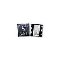
... TriQuint Semiconductor Inc • Phone +1-503-615-9000 • FAX: +1-503-615-8900 • e-mail: info-sales@tqs.com • Web site: www.TriQuint.com Mechanical Information Product Marking The component will be laser marked with a “AP561-F” product label with an alphanumeric lot code on the top surface of the package. Tape and reel specifications for this part will be located on the website in the “Application Notes” ...