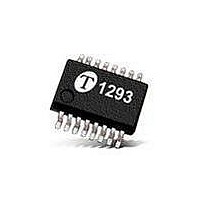
1290Q16-U THAT Corporation, 1290Q16-U Datasheet - Page 5

1290Q16-U
Manufacturer Part Number
1290Q16-U
Description
Difference Amplifiers Dual Bal. Line Receiver 0 db
Manufacturer
THAT Corporation
Datasheet
1.1290Q16-U.pdf
(10 pages)
Specifications of 1290Q16-U
Lead Free Status / RoHS Status
Lead free / RoHS Compliant
THAT 1290 Series
Low Cost Dual Balanced Line Receivers
can unbalance common mode input signals. This can
convert common-mode to balanced signals which will
not be rejected by the CMRR of the devices. For this
reason, THAT recommends dc-coupling the inputs of
the 1290-series devices.
Input Voltage Limitations
input signals above the power supply rails. This is
because the internal opamp’s inputs connect to the
outside world only through the on-chip resistors R
through R
Consider the following analysis.
Differential Input Signals
signal handling will be output clipping. The outputs
of all the devices typically clip at within 2V of the
supply rails. Therefore, maximum differential input
signal levels are directly related to the gain and
supply rails and can be calculated in dBu as follows:
V
V
Gain = -3 dB, then
Common-Mode Input Signals
tially no output signal. The limitation on common-
mode handling is the point at which the inputs are
overloaded. So, we must consider the inputs of the
opamp.
input current splits to flow through both R
R
consider only the voltage at node a.
(R
Furthermore, the same constraints apply to v
the differential analysis.
maximum common-mode input signal for the 1290 is
V
3
in(diff)
in(diff)
/R
3
in(diff)
or
For example, If V
+ R
4
The 1290 series devices are capable of accepting
For differential signals (v
For common-mode input signals, there is essen-
For common-mode signals (V
The voltage at a can be calculated as:
V
Solving for v
V
For the 1290, (R
Following the same reasoning as above, the
.
a
IN(CM)
= 20 log
= 20 log(V
Because V
4
= V
= 20 log[15V − (−15V) − 4V] − (−3dB) − 6.8dB
= 24.5 dBu
) /R
4
= V
IN(CM)
at nodes a and b as shown in Figure 2.
4
= 2.4. For the 1296, (R
a
IN(CM)
V CC −V EE
R
R
b
CC
3
3
R
R
0.775
+R
+R
is constrained to follow V
2
4
4
− V
2
CC
4
4
,
3
=15V, V
−2V
+ R
EE
Tel: +1 508 478 9200; Fax: +1 508 478 0990; Web: www.thatcorp.com
THAT Corporation; 45 Sumner Street; Milford, MA 01757-1656; USA
− Gain
− 4V) − Gain − 6.8dB
4
) /R
IN(DIFF)
EE
IN(CM)
4
=-15V, and
= 2. For the 1293,
), the common-mode
), the limitation to
3
1
/R
+ R
Copyright © 2008, THAT Corporation
2
and through
4
) /R
a
, we will
a
4
as in
= 3.
Page 5 of 10
1
(2V
the 1293, these figures are (2.4V
(2.4V
(3V
rails, the 1290 will accept up to ~26 V in either
direction. As an ac signal, this is 52 V peak-peak,
18.4 V rms, or +27.5 dBu. With the same supply
rails, the 1293 will accept up to ~31 V in either
direction. As an ac signal, this is 62 V peak-peak,
21.9 V rms, or +29 dBu. With the same supply rails,
the 1296 will accept up to ~39 V in either direction.
As an ac signal, this is 78 V peak-peak, 27.6 V rms,
or +31 dBu.
common-mode signals combine. The maximum
signal that can be accommodated will depend on the
superposition of both differential and common-mode
limitations.
Output Considerations
supplying 42 mA into a short circuit. While they will
survive a short, power dissipation will rise dramati-
cally if the output is shorted. Junction temperature
must be kept under 125 ºC to maintain the devices’
specifications.
load capacitance over the entire rated temperature
range, and even more at room temperature.
Power Supply Considerations
tive to the power supply, but they do contain wide
bandwidth opamps. Accordingly, small local bypass
capacitors should be located within a few inches of
the supply pins on these parts, as shown in Figure 4.
Selecting a Gain Variation
structures to suit different applications. The 1296 is
customarily configured for -6 dB gain, but by revers-
ing the resistor connections, it can also be configured
for +6 dB. The 1293 is most often configured for
-3 dB gain, but can also be configured for +3 dB.
The choice of input gain is determined by the input
voltage range to be accommodated, and the power
supply voltages used within the circuit.
ratio, the input stage should be selected and config-
ured for the highest possible gain that will ensure
that maximum-level input signals will not clip the
input stage or succeeding stages. For example, with
±18 V supply rails, the 1290-series parts have a
maximum output signal swing of +23 dBu. In order
to
maximum gain for the stage is -1 dB. With ±15 V
supply rails, the maximum output signal swing is
~+21.1 dBu; here, -3 dB is the maximum gain. In
each case, a 1293 configured for -3 dB gain is the
ideal choice.
CC
CC
accommodate +24
Therefore, for common-mode signals and ±15 V
Of course, in the real world, differential and
The 1290-series devices are typically capable of
These devices are stable with up to 200 pF of
The 1290-series parts are not particularly sensi-
The three different parts offer different gain
To minimize noise and maximize signal-to-noise
EE
- 6) V, and (3V
- 4) V, and the minimum is (2V
+ 4.8) V.
The 1290 (0 dB gain only) will not
For the 1296, these figures are
EE
+ 6) V.
dBu
Document 600121 Rev 01
input signals,
CC
EE
- 4.8) V, and
+ 4) V. For
the


