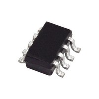
MAX9616AXA+T Maxim Integrated Products, MAX9616AXA+T Datasheet - Page 7

MAX9616AXA+T
Manufacturer Part Number
MAX9616AXA+T
Description
Op Amps LW-POW SNGL/DUAL R-R I/O OP AMPS
Manufacturer
Maxim Integrated Products
Datasheet
1.MAX9614AXTT.pdf
(12 pages)
Specifications of MAX9616AXA+T
Number Of Channels
2
Common Mode Rejection Ratio (min)
78 dB
Input Voltage Range (max)
5.5 V
Input Voltage Range (min)
2.5 V
Input Offset Voltage
17 uV
Input Bias Current (max)
135 pA
Supply Current
170 uA
Maximum Power Dissipation
245 mW
Maximum Operating Temperature
+ 125 C
Minimum Operating Temperature
- 40 C
Mounting Style
SMD/SMT
Slew Rate
1.3 V/us
Package / Case
SC70-8
Lead Free Status / RoHS Status
Lead free / RoHS Compliant
(V
1V/div
1V/div
V
CC
GND
GND
OUT
V
MAX9614
IN
= 3.3V, V
—
—
—
—
—
—
1
2
3
4
5
6
Low-Power Single/Dual, Rail-to-Rail Op Amps
A
V
RECOVERY FROM SATURATION
= 10V/V
OUTPUT SATURATED TO V
PIN
IN+
= V I
MAX9616
_______________________________________________________________________________________
10µs/div
N-
—
—
—
—
3
5
4
2
6
1
7
8
GND
= 0V, V
IN+
IN-
1
2
3
MAX9614-16 toc26
+
CM
CC
= V
NAME
OUTA
OUTB
SHDN
6 SC70
MAX9614
INA+
INB+
GND
INA-
INB-
OUT
V
IN+
IN-
CC
CC
/2, R
L
25
20
15
10
5
0
Typical Operating Characteristics (continued)
= 10kI to V
Positive Input
Positive Input A
Positive Input B
Ground
Negative Input
Negative Input A
Negative Input B
Output
Output A
Output B
Active-Low Shutdown
Positive Power Supply. Bypass with a 0.1FF capacitor to ground.
0
OUTPUT IMPEDANCE vs. FREQUENCY
6
5
4
V
SHDN
OUT
0.1
CC
NOT TO SCALE
TOP VIEW
CC
FREQUENCY (kHz)
1
/2, values are at T
10
100
OUTA
INA+
GND 4
INA-
1000
1
2
3
+
10,000
A
= +25NC, unless otherwise noted.)
FUNCTION
8 SC70
MAX9616
1V/div
1V/div
V
OUT
V
IN
Pin Configuration
8
7
6
5
V
OUTB
INB-
INB+
NO PHASE REVERSAL
CC
Pin Description
200µs/div
MAX9614 toc28
7


