MAX2062ETM+ Maxim Integrated Products, MAX2062ETM+ Datasheet - Page 17
MAX2062ETM+
Manufacturer Part Number
MAX2062ETM+
Description
RF Amplifier DL 50-1000MHZ HI-LIN SER/PARALLEL ANALOG
Manufacturer
Maxim Integrated Products
Datasheet
1.MAX2062ETM.pdf
(24 pages)
Specifications of MAX2062ETM+
Bandwidth
50 MHz to 1000 MHz
Mounting Style
SMD/SMT
Operating Supply Voltage
5 V
Supply Current
148 mA
Maximum Power Dissipation
5.3 W
Maximum Operating Temperature
+ 85 C
Minimum Operating Temperature
- 40 C
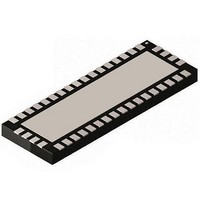
Package / Case
TQFN-48
Lead Free Status / RoHS Status
Lead free / RoHS Compliant


The MAX2062 high-linearity analog/digital VGA is a
general-purpose, high-performance amplifier designed
to interface with 50I systems operating in the 50MHz to
1000MHz frequency range.
Each channel of the device integrates one digital attenua-
tor and one analog attenuator to provide 64dB of total gain
control, as well as a driver amplifier optimized to provide
high gain, high IP3, low NF, and low power consumption.
Each digital attenuator is controlled as a slave periph-
eral using either the SPI-compatible interface, or a 5-bit
parallel bus with 31dB total adjustment range in 1dB
steps. An added feature allows rapid-fire gain selection
among each of the four steps, preprogrammed by the
user through the SPI-compatible interface. A separate
2-pin control lets the user quickly access any one of four
customized attenuation states without reprogramming
the SPI bus. Each analog attenuator is controlled using
an external voltage or through the SPI-compatible inter-
face using an on-chip 8-bit DAC. See the Applications
Information section for attenuator programming details.
Because each of the three stages in the separate signal
paths has its own RF input and RF output, this compo-
nent can be configured to either optimize NF (amplifier
configured first), OIP3 (amplifier last), or a compromise
of NF and OIP3. The device’s performance features
include 24dB amplifier gain (amplifier only), 7.3dB NF
at maximum gain (includes attenuator insertion losses),
PIN
40
41
42
43
44
45
46
47
—
Serial/Parallel-Controlled Analog/Digital VGA
D_ATT_OUT_1
A_ATT_IN_1
______________________________________________________________________________________
NAME
AA_SP
D4_1
D3_1
D2_1
D1_1
D0_1
Dual 50MHz to 1000MHz High-Linearity,
EP
Detailed Description
DAC Enable/Disable Logic Input for Analog Attenuators. Set AA_SP to logic 1 to enable on-chip
DAC circuit and digital SPI control. Set AA_SP to logic 0 to disable DAC circuit and digital SPI
control. When AA_SP = 0, use analog control lines (A_VCTL_1 and A_VCTL_2).
Analog Attenuator Input (50I), Path 1. Requires a DC-blocking capacitor. Connect to
D_ATT_OUT_1 through a 1000pF capacitor.
16dB Attenuator Logic Input, Path 1. Logic 0 = disable, logic 1 = enable.
5-Bit Digital Attenuator Output (50I), Path 1. Requires a DC-blocking capacitor. Connect to
A_ATT_IN_1 through a 1000pF capacitor.
8dB Attenuator Logic Input, Path 1. Logic 0 = disable, logic 1 = enable.
4dB Attenuator Logic Input, Path 1. Logic 0 = disable, logic 1 = enable.
2dB Attenuator Logic Input, Path 1. Logic 0 = disable, logic 1 = enable.
1dB Attenuator Logic Input, Path 1. Logic 0 = disable, logic 1 = enable.
Exposed Pad. Internally connected to GND. Connect to GND for proper RF performance and
enhanced thermal dissipation.
and a high OIP3 level of +41dBm. Each of these features
makes the device an ideal VGA for multipath receiver
and transmitter applications.
In addition, the device operates from a single +5V
supply with full performance, or a +3.3V supply for an
enhanced power-savings mode with lower performance.
The device is available in a compact 48-pin TQFN pack-
age (7mm x 7mm) with an exposed pad. Electrical per-
formance is guaranteed over the extended temperature
range (T
The device integrates two analog attenuators and two
5-bit digital attenuators to achieve a high level of dynam-
ic range. Each analog attenuator has a 33dB range
and is controlled using an external voltage or through
the 3-wire SPI interface using an on-chip 8-bit DAC.
Each digital attenuator has a 31dB control range, a 1dB
step size, and is programmed either through the 3-wire
SPI or through a separate 5-bit parallel bus. See the
Applications Information section and Table 1 for attenu-
ator programming details. The attenuators can be used
for both static and dynamic power control.
Note that when the analog attenuators are controlled
by the DACs through the SPI bus, the DAC output
voltage shows on pins A_VCTL_1 and A_VCTL_2 (pins
39 and 22, respectively). Therefore, in SPI mode, the
A_VCTL_1 and A_VCTL_2 pins must only connect to the
resistor and capacitor to ground, as shown in the Typical
Application Circuit.
Analog and 5-Bit Digital Attenuator Control
FUNCTION
C
= -40NC to +85NC).
Pin Description (continued)
17
Related parts for MAX2062ETM+
Image
Part Number
Description
Manufacturer
Datasheet
Request
R

Part Number:
Description:
MAX7528KCWPMaxim Integrated Products [CMOS Dual 8-Bit Buffered Multiplying DACs]
Manufacturer:
Maxim Integrated Products
Datasheet:
Part Number:
Description:
Single +5V, fully integrated, 1.25Gbps laser diode driver.
Manufacturer:
Maxim Integrated Products
Datasheet:
Part Number:
Description:
Single +5V, fully integrated, 155Mbps laser diode driver.
Manufacturer:
Maxim Integrated Products
Datasheet:
Part Number:
Description:
VRD11/VRD10, K8 Rev F 2/3/4-Phase PWM Controllers with Integrated Dual MOSFET Drivers
Manufacturer:
Maxim Integrated Products
Datasheet:
Part Number:
Description:
Highly Integrated Level 2 SMBus Battery Chargers
Manufacturer:
Maxim Integrated Products
Datasheet:
Part Number:
Description:
Current Monitor and Accumulator with Integrated Sense Resistor; ; Temperature Range: -40°C to +85°C
Manufacturer:
Maxim Integrated Products
Part Number:
Description:
TSSOP 14/A�/RS-485 Transceivers with Integrated 100O/120O Termination Resis
Manufacturer:
Maxim Integrated Products
Part Number:
Description:
TSSOP 14/A�/RS-485 Transceivers with Integrated 100O/120O Termination Resis
Manufacturer:
Maxim Integrated Products
Part Number:
Description:
QFN 16/A�/AC-DC and DC-DC Peak-Current-Mode Converters with Integrated Step
Manufacturer:
Maxim Integrated Products
Part Number:
Description:
TDFN/A/65V, 1A, 600KHZ, SYNCHRONOUS STEP-DOWN REGULATOR WITH INTEGRATED SWI
Manufacturer:
Maxim Integrated Products
Part Number:
Description:
Integrated Temperature Controller f
Manufacturer:
Maxim Integrated Products
Part Number:
Description:
SOT23-6/I�/45MHz to 650MHz, Integrated IF VCOs with Differential Output
Manufacturer:
Maxim Integrated Products
Part Number:
Description:
SOT23-6/I�/45MHz to 650MHz, Integrated IF VCOs with Differential Output
Manufacturer:
Maxim Integrated Products
Part Number:
Description:
EVALUATION KIT/2.4GHZ TO 2.5GHZ 802.11G/B RF TRANSCEIVER WITH INTEGRATED PA
Manufacturer:
Maxim Integrated Products
Part Number:
Description:
QFN/E/DUAL PCIE/SATA HIGH SPEED SWITCH WITH INTEGRATED BIAS RESISTOR
Manufacturer:
Maxim Integrated Products
Datasheet: