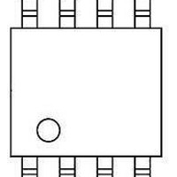
UPC3221GV-A CEL, UPC3221GV-A Datasheet - Page 3

UPC3221GV-A
Manufacturer Part Number
UPC3221GV-A
Description
RF Amplifier Gen Pur AGC Amp
Manufacturer
CEL
Type
RF IC'sr
Datasheet
1.UPC3221GV-E1-A.pdf
(19 pages)
Specifications of UPC3221GV-A
Mounting Style
SMD/SMT
Operating Frequency
10 MHz to 100 MHz
Noise Figure
4.2 dB
Operating Supply Voltage
4.5 V to 5.5 V
Supply Current
33 mA
Maximum Power Dissipation
250 mW
Maximum Operating Temperature
+ 85 C
Minimum Operating Temperature
- 40 C
Package / Case
SSOP-8
Lead Free Status / RoHS Status
Lead free / RoHS Compliant
PIN EXPLANATIONS
Pin
No.
1
2
3
4
5
6
7
8
Note Pin voltage is measured at V
OUTPUT2
OUTPUT1
Pin Name
INPUT1
INPUT2
GND2
GND1
V
V
AGC
CC
4.5 to 5.5
Voltage
0 to V
Applied
(V)
−
−
0
−
−
0
CC
Voltage
(V)
1.29
1.29
2.28
2.28
Pin
−
−
−
−
Note
CC
= 5.0 V.
Power supply pin.
This pin should be externally equipped
with bypass capacitor to minimize
ground impedance.
Signal input pins to AGC amplifier.
This pin should be coupled with
capacitor for DC cut.
Gain control pin.
This pin’s bias govern the AGC output
level.
Recommended to use AGC voltage with
externally resister (example: 1 kΩ).
Ground pin.
This pin should be connected to system
ground with minimum inductance.
Ground pattern on the board should be
formed as wide as possible.
Signal output pins of video amplifier.
This pin should be coupled with
capacitor for DC cut.
Ground pin.
This pin should be connected to system
ground with minimum inductance.
Ground pattern on the board should be
formed as wide as possible.
All ground pins must be connected
together with wide ground pattern to
decrease impedance difference.
Minimum Gain at V
Maximum Gain at V
Data Sheet PU10171EJ03V0DS
Function and Application
AGC
AGC
: 0 to 0.5 V
: 3 to 3.5 V
AGC
Control
4
1
5
1
8
Internal Equivalent Circuit
1
2
⎯⎯⎯
⎯⎯⎯
⎯⎯⎯
5
µ
PC3221GV
7
6
AGC
Amp.
3
3


