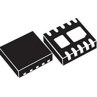
MAX11106ATB+T Maxim Integrated Products, MAX11106ATB+T Datasheet - Page 8

MAX11106ATB+T
Manufacturer Part Number
MAX11106ATB+T
Description
ADC (A/D Converters) 2MSPS/3MSPS LW-PW SER 12/10/8-BIT ADC
Manufacturer
Maxim Integrated Products
Datasheet
1.MAX11117AUTT.pdf
(30 pages)
Specifications of MAX11106ATB+T
Number Of Converters
2
Conversion Rate
3 MSPs
Resolution
10 bit
Interface Type
Serial (3-Wire, SPI, QSPI, Microwire)
Snr
61.8 dB
Voltage Reference
1 V
Supply Voltage (max)
3.6 V
Supply Voltage (min)
2.2 V
Maximum Power Dissipation
1951 mW
Maximum Operating Temperature
+ 125 C
Mounting Style
SMD/SMT
Package / Case
TDFN-10
Input Voltage
2.2 V to 3.6 V
Minimum Operating Temperature
- 40 C
Lead Free Status / RoHS Status
Lead free / RoHS Compliant
ELECTRICAL CHARACTERISTICS (MAX11106) (continued)
(V
unless otherwise noted. Typical values are at T
ELECTRICAL CHARACTERISTICS (MAX11110/MAX11117)
(V
C
2Msps/3Msps, Low-Power,
Serial 12-/10-/8-Bit ADCs
8
POWER SUPPLY
Positive Supply Voltage
Digital I/O Supply Voltage
Positive Supply Current (Full-
Power Mode)
Positive Supply Current (Full-
Power Mode), No Clock
Power-Down Current
Line Rejection
TIMING CHARACTERISTICS (Note 1)
Quiet Time
CS Pulse Width
CS Fall to SCLK Setup
CS Falling Until DOUT High-
Impedance Disabled
Data Access Time After SCLK
Falling Edge (Figure 2)
SCLK Pulse Width Low
SCLK Pulse Width High
Data Hold Time From SCLK
Falling Edge
SCLK Falling Until DOUT High-
Impedance
Power-Up Time
DC ACCURACY
Resolution
Integral Nonlinearity
Differential Nonlinearity
Offset Error
Gain Error
Total Unadjusted Error
DOUT
DD
DD
______________________________________________________________________________________
= 2.2V to 3.6V, V
= 2.2V to 3.6V. MAX11110: f
= 10pF, T
PARAMETER
PARAMETER
A
= -40NC to +125NC, unless otherwise noted. Typical values are at T
REF
= V
DD
, V
SCLK
OVDD
SYMBOL
SYMBOL
V
I
OVDD
I
I
DNL
V
OVDD
TUE
VDD
VDD
INL
I
OE
GE
t
PD
t
t
t
t
t
t
t
t
DD
= 32MHz, 50% duty cycle, 2Msps. MAX11117: f
Q
1
2
3
4
5
6
7
8
= V
DD
A
, f
= +25NC.)
V
V
Leakage only
V
(Note 2)
V
V
Percentage of clock period
Percentage of clock period
Figure 3
Figure 4 (Note 2)
Conversion cycle
No missing codes
MAX11117
MAX11110
Excluding offset and reference errors,
MAX11117
Excluding offset and reference errors,
MAX11110
AIN_
AIN_
DD
OVDD
OVDD
SCLK
= +2.2V to +3.6V,
= V
= V
= 48MHz, 50% duty cycle, 3Msps; C
= 2.2V - 3.6V
= 1.5V - 2.2V
GND
GND
CONDITIONS
CONDITIONS
V
REF
= 2.2V
A
= +25NC.)
SCLK
DOUT
= 48MHz, 50% duty cycle, 3Msps.
MIN
MIN
2.2
1.5
2.5
10
40
40
10
4
5
1
5
= 10pF, T
Q0.15
Q0.5
Q0.3
Q0.7
TYP
1.98
0.17
TYP
1.3
Q1
A
= -40NC to +125NC,
Q1.65
MAX
MAX
0.33
16.5
Q1.2
Q1.4
V
3.6
3.3
10
15
60
60
14
Q1
Q1
Q1
DD
1
UNITS
UNITS
LSB/V
Cycle
LSB
LSB
LSB
LSB
LSB
Bits
mA
mA
FA
ns
ns
ns
ns
ns
ns
ns
%
%
V
V


