TSL2569T TAOS, TSL2569T Datasheet - Page 12
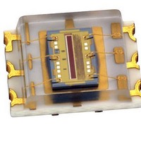
TSL2569T
Manufacturer Part Number
TSL2569T
Description
Light to Digital Converters Light to Digital Sensor
Manufacturer
TAOS
Datasheet
1.TSL2569CS.pdf
(36 pages)
Specifications of TSL2569T
Data Bus Width
20 bit
Peak Wavelength
640 nm, 940 nm
Maximum Operating Frequency
780 KHz
Operating Supply Voltage
2.7 V to 3.6 V
Operating Current
0.6 mA to 15 uA
Maximum Operating Temperature
+ 70 C
Minimum Operating Temperature
- 30 C
Interface Type
I2C
Maximum Fall Time
300 ns
Maximum Rise Time
300 ns
Mounting Style
SMD/SMT
Resolution
16 bit
Package / Case
TMB-6
Lead Free Status / RoHS Status
Lead free / RoHS Compliant


TSL2568, TSL2569
LIGHT-TO-DIGITAL CONVERTER
TAOS091D − DECEMBER 2008
Command Register
NOTE: An I
Control Register (0h)
12
Copyright E 2008, TAOS Inc.
ADDRESS
Reset Value:
Reset Value:
POWER
BLOCK
CLEAR
WORD
FIELD
FIELD
CMD
Resv
The command register specifies the address of the target register for subsequent read and write operations.
The Send Byte protocol is used to configure the COMMAND register. The command register contains eight bits
as described in Table 3. The command register defaults to 00h at power on.
The CONTROL register contains two bits and is primarily used to power the TSL256x device up and down as
shown in Table 4.
SMBus read/write protocol requires a Byte Count. All four ADC Channel Data Registers (Ch through Fh) can be read simultaneously in
a single SMBus transaction. This is the only 32-bit data block supported by the TSL2568 SMBus protocol. The BLOCK bit must be set
to 1, and a read condition should be initiated with a COMMAND CODE of 9Bh. By using a COMMAND CODE of 9Bh during an SMBus
Block Read Protocol, the TSL2568 device will automatically insert the appropriate Byte Count (Byte Count = 4) as illustrated in Figure 15.
A write condition should not be used in conjunction with the Bh register.
0h
2
C block transaction will continue until the Master sends a stop condition. See Figure 14 and Figure 15. Unlike the I
CMD
Resv
BIT
BIT
3:0
7:2
1:0
7
7
6
5
4
7
0
0
Select command register. Must write as 1.
Interrupt clear. Clears any pending interrupt. This bit is a write-one-to-clear bit. It is self clearing.
SMB Write/Read Word Protocol. 1 indicates that this SMB transaction is using either the SMB Write Word or
Read Word protocol.
Block Write/Read Protocol. 1 indicates that this transaction is using either the Block Write or the Block Read
protocol. See Note below.
Register Address. This field selects the specific control or status register for following write and read
commands according to Table 2.
Reserved. Write as 0.
Power up/power down. By writing a 03h to this register, the device is powered up. By writing a 00h to this
register, the device is powered down.
NOTE: If a value of 03h is written, the value returned during a read cycle will be 03h. This feature can be
used to verify that the device is communicating properly.
CLEAR
Resv
6
0
6
0
WORD
Resv
0
0
5
5
r
Table 3. Command Register
Table 4. Control Register
www.taosinc.com
BLOCK
Resv
4
4
0
0
Resv
0
0
3
3
DESCRIPTION
DESCRIPTION
Resv
2
2
0
0
ADDRESS
r
1
0
1
0
POWER
The LUMENOLOGY r Company
0
0
0
0
2
C protocol, the
COMMAND
CONTROL
Related parts for TSL2569T
Image
Part Number
Description
Manufacturer
Datasheet
Request
R

Part Number:
Description:
Microcontroller Modules & Accessories TAOS Eval Module w/USB Interface
Manufacturer:
TAOS
Part Number:
Description:
Optical Sensor Development Tools TAOS Eval Module
Manufacturer:
TAOS

Part Number:
Description:
Industrial Optical Sensors Ambient Light Sensor SMBus
Manufacturer:
TAOS
Datasheet:

Part Number:
Description:
Photodiodes TriColor Sensor RGB, Clear Ch
Manufacturer:
TAOS
Datasheet:

Part Number:
Description:
LED Displays Hexadecimal Display 4-bit
Manufacturer:
TAOS
Datasheet:

Part Number:
Description:
Photodiodes Linear Sensor Array 200dpi 64pix
Manufacturer:
TAOS
Datasheet:

Part Number:
Description:
Industrial Optical Sensors Ambient Light Sensor SMBus
Manufacturer:
TAOS
Datasheet:

Part Number:
Description:
Photodiodes Linear Array 200 DPI
Manufacturer:
TAOS
Datasheet:

Part Number:
Description:
Photodiodes Light to Voltage Converter
Manufacturer:
TAOS
Datasheet:

Part Number:
Description:
Photodiodes Linear Array 200 DPI
Manufacturer:
TAOS
Datasheet:
Part Number:
Description:
Industrial Optical Sensors Ambient Light Sensor SMBus
Manufacturer:
TAOS
Datasheet:
Part Number:
Description:
Photodiodes TriColor Sensor RGB, Clear Ch
Manufacturer:
TAOS
Datasheet:
Part Number:
Description:
LED Displays Hexadecimal Display 4-bit
Manufacturer:
TAOS
Datasheet:
Part Number:
Description:
Photodiodes Linear Sensor Array 200dpi 64pix
Manufacturer:
TAOS
Datasheet:
