ZVN3310A Diodes Inc, ZVN3310A Datasheet
Home Integrated Circuits (ICs) MOSFET Small Signal ZVN3310A
Manufacturer Part Number
ZVN3310A
Description
MOSFET Small Signal N-Chnl 100V
Specifications of ZVN3310A
Minimum Operating Temperature
- 55 C
Configuration
Single
Transistor Polarity
N-Channel
Resistance Drain-source Rds (on)
10 Ohm @ 10 V
Drain-source Breakdown Voltage
100 V
Gate-source Breakdown Voltage
+/- 20 V
Continuous Drain Current
0.2 A
Power Dissipation
625 mW
Maximum Operating Temperature
+ 150 C
Mounting Style
Through Hole
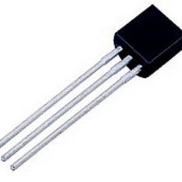
Package / Case
E-Line
Lead Free Status / RoHS Status
Lead free / RoHS Compliant
Lead Free Status / RoHS Status
Lead free / RoHS Compliant
Available stocks
N-CHANNEL ENHANCEMENT
MODE VERTICAL DMOS FET
ISSUE 2 – MARCH 94
FEATURES
*
*
ABSOLUTE MAXIMUM RATINGS.
ELECTRICAL CHARACTERISTICS (at T
PARAMETER
Drain-Source Voltage
PARAMETER
Drain-Source Breakdown
Voltage
Gate-Body Leakage
On-State Drain Current(1)
Continuous Drain Current at T
Pulsed Drain Current
Gate-Source Voltage
Power Dissipation at T
Operating and Storage Temperature Range
Gate-Source Threshold
Voltage
Zero Gate Voltage Drain
Current
Static Drain-Source On-State
Resistance (1)
Forward Transconductance(1)(2
)
Input Capacitance (2)
Common Source Output
Capacitance (2)
Reverse Transfer Capacitance
(2)
Turn-On Delay Time (2)(3)
Rise Time (2)(3)
Turn-Off Delay Time (2)(3)
Fall Time (2)(3)
100 Volt V
R
DS(on)
= 10
DS
amb
=25°C
amb
SYMBOL MIN.
BV
V
I
I
I
R
g
C
C
C
t
t
t
t
GSS
DSS
D(on)
d(on)
r
d(off)
f
=25°C
fs
GS(th)
DS(on)
iss
oss
rss
DSS
100
0.8
500
100
3-378
amb
SYMBOL
V
I
I
V
P
T
D
DM
tot
j
DS
GS
= 25°C unless otherwise stated).
:T
MAX. UNIT CONDITIONS.
2.4
20
1
50
10
40
15
5
5
7
6
7
stg
V
V
nA
mA
mS
pF
pF
pF
ns
ns
ns
ns
A
A
I
ID=1mA, V
V
V
V
V
V
V
V
V
D
GS
DS
DS
DS
GS
DS
DS
DD
=1mA, V
-55 to +150
=100V, V
=80V, V
=25V, V
=25V,I
=25V, V
= 20V, V
=10V,I
VALUE
25V, I
100
200
625
ZVN3310A
2
20
TO92 Compatible
D
D
GS
DS
=500mA
=500mA
GS
GS
GS
D
D
G
=0V
GS
=500mA
= V
DS
=0V, T=125°C
=10V
=0V, f=1MHz
S
E-Line
=0
=0V
GS
UNIT
mW
mA
°C
V
A
V
(2)
Related parts for ZVN3310A
ZVN3310A Summary of contents
... V GS(th GSS I 1 DSS 50 I 500 mA D(on DS(on) g 100 iss oss rss d(on d(off 3-378 ZVN3310A E-Line TO92 Compatible VALUE UNIT 100 200 625 mW -55 to +150 °C I =1mA ID=1mA 20V =100V =80V, V =0V, T=125° =25V, V =10V =10V,I =500mA GS ...
... Transfer Characteristics 2.4 2.2 2.0 1.8 1.6 1 1.2 1A 1.0 0.5A 0.2A 0.8 0.6 0.4 -80 -60 -40 - Normalised R 3-379 ZVN3310A Drain Source Voltage (Volts Gate Source Voltage (Volts) GS- I 0.5A D=- 100 120 140 160 T-Temperature (C°) and V vs Temperature DS(on) GS(th) V GS= 10V ...
... ZVN3310A TYPICAL CHARACTERISTICS 160 120 0.2 0.4 0.6 0 Drain Current (Amps) D Transconductance v drain current -Drain Source Voltage (Volts) DS Capacitance v drain-source voltage 160 V 25V DS= 120 1.0 1.2 0 Transconductance v gate-source voltage iss oss 2 C rss 0.1 0.2 0.3 0.4 0.5 0.6 0.7 0.8 0.9 1.0 1.1 1.2 ...
Related keywords
ZVN3310A datasheet ZVN3310A data sheet ZVN3310A pdf datasheet ZVN3310A component ZVN3310A part ZVN3310A distributor ZVN3310A RoHS ZVN3310A datasheet download