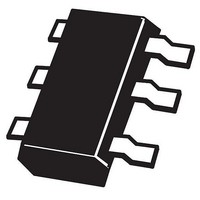
ZVP4525E6TA Diodes Inc, ZVP4525E6TA Datasheet
Home Integrated Circuits (ICs) MOSFET Small Signal ZVP4525E6TA
Manufacturer Part Number
ZVP4525E6TA
Description
MOSFET Small Signal P-Chnl 250V
Specifications of ZVP4525E6TA
Minimum Operating Temperature
- 55 C
Configuration
Single Quad Drain
Transistor Polarity
P-Channel
Resistance Drain-source Rds (on)
14 Ohm @ 10 V
Drain-source Breakdown Voltage
250 V
Gate-source Breakdown Voltage
+/- 40 V
Continuous Drain Current
0.197 A
Power Dissipation
1100 mW
Maximum Operating Temperature
+ 150 C
Mounting Style
SMD/SMT
Package / Case
SOT-23
Lead Free Status / RoHS Status
Lead free / RoHS Compliant
Lead Free Status / RoHS Status
Lead free / RoHS Compliant
Available stocks
ISSUE 1 - MARCH 2001
250V P-CHANNEL ENHANCEMENT MODE MOSFET
SUMMARY
DESCRIPTION
This 250V enhancement mode P-channel MOSFET provides users with a
competitive specification offering efficient power handling capability, high
impedance and is free from thermal runaway and thermally induced
secondary breakdown. Applications benefiting from this device include a
variety of Telecom and general high voltage circuits.
SOT89 and SOT223 versions are also available.
FEATURES
APPLICATIONS
ORDERING INFORMATION
DEVICE MARKING
DEVICE
ZVP4525TA
ZVP4525TC
(
High voltage
Low on-resistance
Fast switching speed
Low gate drive
Low threshold
Complementary N-channel Type ZVN4525E6
SOT23-6 package
Earth Recall and dialling switches
Electronic hook switches
High Voltage Power MOSFET Drivers
Telecom call routers
Solid state relays
P52
REEL SIZE
(inches)
13
7
TAPE WIDTH (mm)
8mm embossed
8mm embossed
1
QUANTITY
PER REEL
3000 units
10000 units
ZVP4525E6
Top View
SOT23-6
Related parts for ZVP4525E6TA
ZVP4525E6TA Summary of contents
P-CHANNEL ENHANCEMENT MODE MOSFET SUMMARY ( DESCRIPTION This 250V enhancement mode P-channel MOSFET provides users with a competitive specification offering efficient power handling capability, high impedance and is free from thermal runaway and thermally induced secondary breakdown. Applications benefiting ...
ZVP4525E6 ABSOLUTE MAXIMUM RATINGS. PARAMETER Drain-Source Voltage Gate Source Voltage Continuous Drain Current (V =10V; TA=25°C)( =10V; TA=70°C)(a) GS Pulsed Drain Current (c) Continuous Source Current (Body Diode) Pulsed Source Current (Body Diode) Power Dissipation at T =25°C ...
ISSUE 1 - MARCH 2001 CHARACTERISTICS 3 ZVP4525E6 ...
ZVP4525E6 ELECTRICAL CHARACTERISTICS (at T PARAMETER STATIC Drain-Source Breakdown Voltage Zero Gate Voltage Drain Current Gate-Body Leakage Gate-Source Threshold Voltage Static Drain-Source On-State Resistance (1) Forward Transconductance (3) DYNAMIC (3) Input Capacitance Output Capacitance Reverse Transfer Capacitance SWITCHING(2) (3) Turn-On ...
TYPICAL CHARACTERISTICS ISSUE 1 - MARCH 2001 ZVP4525E6 5 ...
ZVP4525E6 CHARACTERISTICS 6 ISSUE 1 - MARCH 2001 ...
TEST CIRCUITS ISSUE 1 - MARCH 2001 ZVP4525E6 7 ...
ZVP4525E6 PACKAGE DIMENSIONS DIM Millimetres Inches Min Max Min A 0.90 1.45 0.35 A1 0.00 0. 0.90 1.30 0.035 b 0.35 0.50 0.014 C 0.09 0.20 0.0035 D 2.80 3.00 ...
Related keywords
ZVP4525E6TA datasheet ZVP4525E6TA data sheet ZVP4525E6TA pdf datasheet ZVP4525E6TA component ZVP4525E6TA part ZVP4525E6TA distributor ZVP4525E6TA RoHS ZVP4525E6TA datasheet download


