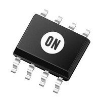
NCP3126ADR2G ON Semiconductor, NCP3126ADR2G Datasheet - Page 13

NCP3126ADR2G
Manufacturer Part Number
NCP3126ADR2G
Description
DC/DC Switching Converters 3A PWM Switching Buck Regulator
Manufacturer
ON Semiconductor
Datasheet
1.NCP3126ADR2G.pdf
(23 pages)
Specifications of NCP3126ADR2G
Mounting Style
SMD/SMT
Duty Cycle (max)
80 %
Efficiency
93 %
Input / Supply Voltage (max)
13.2 V
Input / Supply Voltage (min)
4.5 V
Maximum Operating Temperature
+ 125 C
Minimum Operating Temperature
- 40 C
Operating Temperature Range
- 40 C to + 125 C
Output Current
3 A
Output Voltage
Adjustable
Supply Current
10 mA
Switching Frequency
350 KHz
Package / Case
SOIC-8
Lead Free Status / RoHS Status
Lead free / RoHS Compliant
Available stocks
Company
Part Number
Manufacturer
Quantity
Price
Company:
Part Number:
NCP3126ADR2G
Manufacturer:
ON
Quantity:
2 500
When calculating the rise time and fall time of the high side
MOSFET it is important to know the charge characteristic
shown in Figure 22.
I
Q
R
R
t
V
V
I
Q
R
R
t
V
V
by both the high−side and low−side MOSFETs, but are
dissipated only in the high−side MOSFET.
C
F
P
V
body diode in the low−side MOSFET is shown as follows:
Vth
RISE
FALL
G1
G2
SW
DS
t
GD
HSPU
G
BST
TH
t
GD
G
HSPD
BST
TH
OSS
IN
RISE
Next, the MOSFET output capacitance losses are caused
Finally, the loss due to the reverse recovery time of the
FALL
Figure 22. MOSFET Switching Characteristics
+
+
Q
Q
I
I
G1
G2
GD
GD
= Output current from the high−side gate
= MOSFET gate to drain gate charge
= Drive pull up resistance
= MOSFET gate resistance
= MOSFET rise time
= Boost voltage
= MOSFET gate threshold voltage
= Output current from the low−side gate drive
= MOSFET gate to drain gate charge
= MOSFET gate resistance
= Drive pull down resistance
= MOSFET fall time
= Boost voltage
= MOSFET gate threshold voltage
= MOSFET output capacitance at 0V
= Switching frequency
= MOSFET drain to source charge losses
= Input voltage
+
+
P
DS
drive
P
V
V
RR
+ 1
BST
BST
+ Q
2
* V
* V
@ C
RR
OSS
TH
TH
@ V
Q
Q
GD
@ V
GD
IN
R
R
HSPU
HSPD
IN
@ F
2
@ F
SW
) R
) R
SW
G
G
(eq. 26)
(eq. 27)
(eq. 28)
(eq. 29)
http://onsemi.com
13
F
P
Q
V
voltages so switching losses are negligible. The low−side
MOSFET’s power dissipation only consists of conduction
loss due to R
non−overlap periods.
P
P
P
follows:
I
R
P
D
I
I
ra
The body diode losses can be approximated as:
F
I
NOL
NOL
P
V
Control Dissipation
The control portion of the IC power dissipation is
determined by the formula below:
I
P
V
designer can calculate the required thermal impedance to
maintain a specified junction temperature at the worst case
RMS_LS
OUT
RMS_LS
OUT
CC
SW
RR
BODY
COND
D_LS
COND
SW
BODY
C
DS(on)_LS
P
RR
IN
FD
IN
The low−side MOSFET turns on into small negative
Conduction loss in the low−side MOSFET is described as
Once the IC power dissipations are determined, the
BODY
I
RMS_LS
HL
LH
+ V
P
COND
+ I
P
FD
= Switching frequency
= High side MOSFET reverse recovery losses
= Reverse recovery charge
= Input voltage
= Low side MOSFET body diode losses
= Low side MOSFET conduction losses
= Low side MOSFET losses
= RMS current in the low side
= Low−side MOSFET on resistance
= High side MOSFET conduction losses
= Duty ratio
= Load current
= RMS current in the low side
= Ripple current ratio
= Switching frequency
= Load current
= Dead time between the high−side
= Dead time between the low−side
= Low−side MOSFET body diode losses
= Body diode forward voltage drop
D_LS
DS(on)
OUT
@ I
+ I
MOSFET turning off and the low−side
MOSFET turning on, typically 50 ns
MOSFET turning off and the high−side
MOSFET turning on, typically 50 ns
= Control circuitry current draw
= Control power dissipation
= Input voltage
OUT
+ P
@
P
RMS_LS
C
@ F
and body diode loss during the
COND
+ I
( 1 * D ) @ 1 ) ra
SW
CC
@ NOL
2
) P
@ R
V
BODY
DS(on)_LS
IN
LH
) NOL
12
2
HL
(eq. 30)
(eq. 31)
(eq. 32)
(eq. 33)
(eq. 34)


