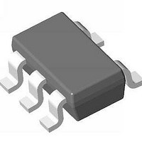
AAT4900IGV-T1 Analogic Tech, AAT4900IGV-T1 Datasheet - Page 9

AAT4900IGV-T1
Manufacturer Part Number
AAT4900IGV-T1
Description
MOSFET & Power Driver ICs Buffered Power Half-Bridge
Manufacturer
Analogic Tech
Type
Buffered Power Half-Bridger
Datasheet
1.AAT4900IGV-T1.pdf
(13 pages)
Specifications of AAT4900IGV-T1
Product
Half-Bridge Drivers
Rise Time
5 ns
Fall Time
5 ns
Supply Voltage (max)
6 V
Supply Voltage (min)
- 0.3 V
Supply Current
4 mA
Maximum Power Dissipation
526 mW
Maximum Operating Temperature
+ 85 C
Mounting Style
SMD/SMT
Bridge Type
Half Bridge
Maximum Turn-on Delay Time
40 ns
Minimum Operating Temperature
- 40 C
Number Of Drivers
1
Number Of Outputs
1
Output Voltage
6.3 V
Package / Case
SOT-23-5
Lead Free Status / RoHS Status
Lead free / RoHS Compliant
Available stocks
Company
Part Number
Manufacturer
Quantity
Price
Company:
Part Number:
AAT4900IGV-T1
Manufacturer:
ATMEL
Quantity:
1 200
Company:
Part Number:
AAT4900IGV-T1
Manufacturer:
AnalogicTech
Quantity:
1 937
Gate Drive
When used as a MOSFET gate driver, the break-
before-make shoot-through protection significantly
reduces losses associated with the driver at high
frequencies. (See Figure 2.)
The low R
high peak gate current and fast switching speeds.
A small package size facilitates close placement to
the power device for optimum switching perform-
ance. The logic level inputs (CLK and EN) are high
impedance inputs.
Gate Drive Current Ratings
An estimate of the maximum gate drive capability
with no external series resistor can be derived from
Equation 7. Note that the quiescent current varies
with the ambient temperature, frequency of opera-
tion, and input voltage. The graphs below display
the quiescent current and maximum gate charge
drive capability at 85°C ambient vs. frequency for
various input voltages.
Eq. 7:
4900.2006.05.1.3
Q
G(MAX)
DS(ON)
=
=
= 40nC
1MHz
F
1
of the output stage allows for a
S
1
·
⎛
⎝
·
T
θ
⎛
⎝
190°C/W · 4.2V
J(MAX)
JA
120°C - 85°C
· V
- T
IN(MAX)
Figure 2: AAT4900 Gate Drive Configuration.
AMB
Enable
Clock
Ground
- I
Q
⎞
⎠
- 3.2mA
EN
CLK
⎞
⎠
AAT4900
GND
+5V
IN
LX
The quiescent current was first measured over
temperature for various input voltages with no load
attached. Equation 7 was then used to derive the
maximum gate charge capability for the desired
maximum junction temperature. Q
charge required to raise the gate of the load MOS-
FET to the input voltage. This value is taken from
the MOSFET manufacturer's gate charge curve.
100
0.1
1000
10
100
1
No Load Operating Current at 85°C Ambient
100
10
1
100
V
Circuit
Load
Maximum Gate Charge Load @ 85°C
Buffered Power Half-Bridge
IN
= 5.5V
(Ambient T
V
IN
= 5.0V
Frequency (kHz)
Frequency (kHz)
V
V
IN
1000
J(MAX)
1000
IN
= 2.7V
= 5.0V
V
V
IN
IN
= 120°C)
= 4.2V
= 5.5V
V
AAT4900
IN
= 4.2V
G
V
IN
is the gate
= 2.7V
10000
10000
9


