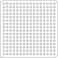
LFXP10C-4FN256C Lattice, LFXP10C-4FN256C Datasheet - Page 11

LFXP10C-4FN256C
Manufacturer Part Number
LFXP10C-4FN256C
Description
FPGA - Field Programmable Gate Array 9.7K LUTs 188 I/O 1.8/2.5/3.3V -4 Spd
Manufacturer
Lattice
Specifications of LFXP10C-4FN256C
Number Of Programmable I/os
188
Data Ram Size
221184
Supply Voltage (max)
3.465 V
Maximum Operating Temperature
+ 85 C
Minimum Operating Temperature
0 C
Mounting Style
SMD/SMT
Supply Voltage (min)
1.71 V
Package / Case
FPBGA-256
Lead Free Status / RoHS Status
Lead free / RoHS Compliant
Available stocks
Company
Part Number
Manufacturer
Quantity
Price
Company:
Part Number:
LFXP10C-4FN256C
Manufacturer:
LATTICE
Quantity:
73
Company:
Part Number:
LFXP10C-4FN256C
Manufacturer:
Lattice Semiconductor Corporation
Quantity:
10 000
- Current page: 11 of 130
- Download datasheet (2Mb)
Lattice Semiconductor
Figure 2-6. Secondary Clock Sources
Clock Routing
The clock routing structure in LatticeXP devices consists of four Primary Clock lines and a Secondary Clock net-
work per quadrant. The primary clocks are generated from MUXs located in each quadrant. Figure 2-7 shows this
clock routing. The four secondary clocks are generated from MUXs located in each quadrant as shown in Figure 2-
8. Each slice derives its clock from the primary clock lines, secondary clock lines and routing as shown in Figure 2-
9.
Figure 2-7. Per Quadrant Primary Clock Selection
Clock Input
From Routing
From Routing
From Routing
From Routing
1. Smaller devices have fewer PLL related lines.
2. Dynamic clock select.
4 Primary Clocks (CLK0, CLK1, CLK2, CLK3) per Quadrant
20 Primary Clock Sources: 12 PLLs + 4 PIOs + 4 Routing
Routing
Routing
From
From
Routing
Routing
20 Secondary Clock Sources
To Quadrant Clock Selection
From
From
Clock
Clock
Input
Input
DCS
2-8
2
Routing
Routing
From
From
Routing
Routing
From
From
LatticeXP Family Data Sheet
DCS
1
2
From Routing
From Routing
From Routing
From Routing
Clock Input
Architecture
Related parts for LFXP10C-4FN256C
Image
Part Number
Description
Manufacturer
Datasheet
Request
R

Part Number:
Description:
FPGA - Field Programmable Gate Array 9.7K LUTs 244 IO 1.8 /2.5/3.3V -4 Spd I
Manufacturer:
Lattice

Part Number:
Description:
FPGA - Field Programmable Gate Array 9.7K LUTs 188 IO 1.8 /2.5/3.3V -3 Spd I
Manufacturer:
Lattice
Datasheet:

Part Number:
Description:
FPGA - Field Programmable Gate Array 9.7K LUTS 188 I/O
Manufacturer:
Lattice
Datasheet:
Part Number:
Description:
FPGA LatticeXP Family 10000 Cells 320MHz 130nm (CMOS) Technology 1.8V/2.5V/3.3V 256-Pin FBGA Tray
Manufacturer:
LATTICE SEMICONDUCTOR
Datasheet:
Part Number:
Description:
FPGA LatticeXP Family 10000 Cells 360MHz 130nm (CMOS) Technology 1.8V/2.5V/3.3V 256-Pin FBGA Tray
Manufacturer:
LATTICE SEMICONDUCTOR
Datasheet:
Part Number:
Description:
FPGA LatticeXP Family 10000 Cells 320MHz 130nm (CMOS) Technology 1.8V/2.5V/3.3V 388-Pin FBGA Tray
Manufacturer:
LATTICE SEMICONDUCTOR
Datasheet:
Part Number:
Description:
FPGA LatticeXP Family 10000 Cells 400MHz 130nm (CMOS) Technology 1.8V/2.5V/3.3V 256-Pin FBGA Tray
Manufacturer:
LATTICE SEMICONDUCTOR
Datasheet:
Part Number:
Description:
FPGA LatticeXP Family 10000 Cells 400MHz 130nm (CMOS) Technology 1.8V/2.5V/3.3V 388-Pin FBGA Tray
Manufacturer:
LATTICE SEMICONDUCTOR
Datasheet:

Part Number:
Description:
FPGA LatticeXP Family 10000 Cells 320MHz 130nm (CMOS) Technology 1.8V/2.5V/3.3V 388-Pin FBGA Tray
Manufacturer:
Lattice
Datasheet:

Part Number:
Description:
IC FPGA 9.7KLUTS 188I/O 256-BGA
Manufacturer:
Lattice
Datasheet:

Part Number:
Description:
IC FPGA 9.7KLUTS 244I/O 388-BGA
Manufacturer:
Lattice
Datasheet:

Part Number:
Description:
IC FPGA 9.7KLUTS 244I/O 388-BGA
Manufacturer:
Lattice
Datasheet:

Part Number:
Description:
IC FPGA 9.7KLUTS 244I/O 388-BGA
Manufacturer:
Lattice
Datasheet:

Part Number:
Description:
IC FPGA 9.7KLUTS 244I/O 388-BGA
Manufacturer:
Lattice
Datasheet:


