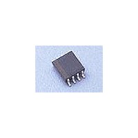
DG419BDQ-T1-E3 Vishay, DG419BDQ-T1-E3 Datasheet - Page 9

DG419BDQ-T1-E3
Manufacturer Part Number
DG419BDQ-T1-E3
Description
Analog Switch ICs Single SPDT 20/25V
Manufacturer
Vishay
Type
Analog Switchr
Specifications of DG419BDQ-T1-E3
Number Of Switches
Single
Switch Configuration
SPDT
On Resistance (max)
35 Ohms @ 12 V
On Time (max)
125 ns @ 12 V
Off Time (max)
66 ns @ 12 V
Off Isolation (typ)
- 82 dB
Supply Voltage (max)
25 V
Supply Current
0.000001 mA @ +/- 16.5 V
Maximum Power Dissipation
400 mW
Maximum Operating Temperature
+ 85 C
Mounting Style
SMD/SMT
Package / Case
MSOP
Minimum Operating Temperature
- 40 C
Off State Leakage Current (max)
12 nA
Propagation Delay Time
87 ns @ +/- 15V/119 ns @ 12V
Analog Switch Type
SPDT
No. Of Channels
1
On State Resistance Max
15ohm
Turn Off Time
38ns
Turn On Time
100ns
Supply Voltage Range
10.8V To 13.2V
Package
8MSOP
Maximum On Resistance
35@10.8V Ohm
Maximum Propagation Delay Bus To Bus
87@±15V|119@12V ns
Maximum High Level Output Current
30 mA
Number Of Channels Per Chip
1
Maximum Turn-off Time
80@±15V ns
Maximum Turn-on Time
125@12V ns
Switch Architecture
SPDT
Power Supply Type
Single|Dual
Lead Free Status / RoHS Status
Lead free / RoHS Compliant
Lead Free Status / RoHS Status
Lead free / RoHS Compliant, Lead free / RoHS Compliant
TEST CIRCUITS
APPLICATIONS
Switched Signal Powers Analog Switch
The analog switch in Figure 10 derives power from its input
signal, provided the input signal amplitude exceeds 4 V and
its frequency exceeds 1 kHz.
This circuit is useful when signals have to be routed to either
of two remote loads. Only three conductors are required: one
for the signal to be switched, one for the control signal and a
common return.
Document Number: 70051
S10-1528-Rev. G, 19-Jul-10
0 V, 2.4 V
0 V, 2.4 V
C
C
DG417/418
IN
IN
+ 5 V
GND
GND
V
V
L
L
+ 15 V
- 15 V
V-
V+
D
D
S
S
Figure 10. Switched Signal Powers Remote SPDT Analog Switch
Control
Input
C
C
C
C
D
1
Figure 9. Source/Drain Capacitances
D
IN
or Equivalent
Impedance
GND
HP4192A
f = 1 MHz
f = 1 MHz
Analyzer
V+
Meter
DG419
V
V-
L
S
S
1
2
0 V, 2.4 V
0 V, 2.4 V
A positive input pulse turns on the clamping diode D
charges C
chip; operation is satisfactory because the switch requires
less than 1 µA of stand-by supply current. Loading of the
signal source is imperceptible. The DG419’s on-resistance is
a low 100 for a 5 V input signal.
C
C
R
10
C
0.01 µF
L1
1
+ 15 V
IN
IN
k
DG419
1
. The charge stored on C
GND
GND
V+
V+
D
D
S
S
2
2
2
2
R
10
DG417, DG418, DG419
NC
NC
L2
k
V
OUT
- 15 V
V-
S
S
D
D
1
1
1
1
C
C
Vishay Siliconix
1
is used to power the
or Equivalent
or Equivalent
www.vishay.com
Impedance
Impedance
HP4192A
HP4192A
f = 1 MHz
f = 1 MHz
Analyzer
Analyzer
Meter
Meter
1
and
9


