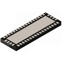
MAX14978ETO+ Maxim Integrated Products, MAX14978ETO+ Datasheet - Page 4

MAX14978ETO+
Manufacturer Part Number
MAX14978ETO+
Description
Analog Switch ICs USB 2.0/3.0 SWITCH High BW LVDS Switch
Manufacturer
Maxim Integrated Products
Datasheet
1.MAX14978ETO.pdf
(15 pages)
Specifications of MAX14978ETO+
On Resistance (max)
10 Ohms
On Time (max)
250 ns
Off Time (max)
50 ns
Off Isolation (typ)
- 17 dB
Bandwidth
950 MHz
Supply Voltage (max)
5.5 V
Supply Voltage (min)
3 V
Supply Current
60 uA
Maximum Power Dissipation
2857 mW
Maximum Operating Temperature
+ 85 C
Mounting Style
SMD/SMT
Package / Case
TQFN-42
Off State Leakage Current (max)
250 nA
Propagation Delay Time
100 ps
Lead Free Status / RoHS Status
Lead free / RoHS Compliant
SuperSpeed USB Passive Switch
(Low/Full/Hi/SuperSpeed)
ELECTRICAL CHARACTERISTICS (continued)
(V
T
4
Crosstalk (Note 7)
Signaling Data Rate
LOGIC INPUT
Input Logic-High
Input Logic-Low
Input Leakage Current
Input Logic Hysteresis
DYNAMIC PERFORMANCE
Turn-On Time
Turn-Off Time
Propagation Delay
Output Skew Between Switches
Output Skew Between Pairs
Output Skew Between Same Pair
Fault-Protection Response Time
A
CC
= +25NC.) (Note 2)
= +3.0V to +5.5V, V
PARAMETER
DD
= +3.0V to +3.6V, T
t
SYMBOL
PLH
V
t
t
t
V
V
HYST
t
V
OFF
t
SK1
SK2
BR
t
I
ON
SK
FP
CT
IN
, t
IH
IL
PHL
A
= -40NC to +85NC, unless otherwise noted. Typical values are at V
Hi-Speed USB switches,
V
R
SuperSpeed USB switch-
es, crosstalk between any
two pairs,
R
anced, Figure 1
SuperSpeed USB switches, R
Hi-Speed USB switches
SuperSpeed USB switches,
V
SuperSpeed USB switches
Hi-Speed USB switches,
V
C
SuperSpeed USB switches,
V
V
C
SuperSpeed USB switches,
V
Hi-Speed USB switches, R
Figure 3
SuperSpeed USB switches, R
Hi-Speed USB switches, skew between
switch 1 and 2, R
SuperSpeed USB switches, R
unbalanced; skew between any two pairs,
Figure 3
SuperSpeed USB switches, R
unbalanced; skew between two lines on
same pair, Figure 3
Hi-Speed USB switches,
V
V
NOD_
L
S
SEL2
NOD
NO_
NOD_
NO_
COMD_ =
CC
L
L
= R
= R
= 35pF, V
= 35pF, V
= 3.3V, Figure 4
_ or V
or V
or V
= 0V or V
, V
S
L
or V
= 50I, Figure 1
= 50I, unbal-
NCD_
NC_
NC_
0V to 5V step, R
NCD_
NCD_
EN
EN
= 1.0V, R
= 1.0V, R
= 0dBm,
CONDITIONS
DD
= V
= 0V to V
= 1.5V, R
= 1.5V, R
L
= R
CC
S
to 0V, Figure 2
L
L
= 50I, Figure 3
= 50I, Figure 2
= 50I, Figure 2
CC
L
L
L
L
f = 10MHz
f = 250MHz
f = 500MHz
f = 50MHz
f = 1.25GHz
= 300I,
= R
= 300I,
, Figure 2
= R
S
S
S
L
= R
= R
= R
= R
S
S
= 50I,
L
L
= 50I,
S
L
= 50I,
= 50I,
= 50I
= 50I
-250
MIN
1.4
0.5
-1
TYP
100
100
-73
-54
-33
-53
-32
5.0
20
90
10
50
40
50
10
1
CC
MAX
+250
100
250
0.5
5.0
+1
50
5
= V
DD
= +3.3V,
UNITS
Gbps
mV
dB
nA
FA
Fs
ns
Fs
ns
ps
ps
ps
ps
Fs
V
V


