EMIF06-MSD02C3 STMicroelectronics, EMIF06-MSD02C3 Datasheet
EMIF06-MSD02C3
Specifications of EMIF06-MSD02C3
Available stocks


Related parts for EMIF06-MSD02C3


EMIF06-MSD02C3 Summary of contents
Page 1
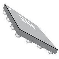
... Figure 1. Pin configuration (bump side Description The EMIF06-mSD02C3 is a highly integrated device based on IPAD technology offering two functions: ESD protection to comply with IEC standard, and EMI filtering to reject mobile phone frequencies. TM: IPAD is a trademark of STMicroelectronics Doc ID 16910 Rev 1 Flip Chip (16 bumps) ...
Page 2
... ESD discharge IEC 61000-4-2, air discharge V PP ESD discharge IEC 61000-4-2, contact discharge V Maximum input voltage in T Maximum junction temperature j T Operating temperature range op T Storage temperature range stg Figure 2. EMIF06-mSD02C3 configuration Clk CMD Data0 HOST Data1 Data2 Data3/CD Table 2. Pin configuration Pin ...
Page 3
... EMIF06-mSD02C3 Table 3. Electrical characteristic Symbol R1, R2, R3, R4, R5, R6 Tolerance ± R10, R11, R12, R13 Tolerance ± Tolerance ± MHz, V line Figure 3. S21 attenuation measurements dB 0.00 - 10.00 - 20.00 - 30.00 - 40.00 - 50.00 F (Hz BIAS - 60.00 100.0k 1.0M 10.0M DATA0 DATA2 CMD Figure 5. ESD response to IEC 61000-4-2 ...
Page 4
... Direct input on 50Ω Input Line “A” Output line “B” 50 50Ω SDData0 Clk Doc ID 16910 Rev 1 EMIF06-mSD02C3 ESD response to IEC 61000-4-2 (-15 kV air discharge 100 ns/div LeCroy Wavesurfer 64Xs 600 MHz – 2.5Gs/s Oscilloscope Voltage Probe ...
Page 5
... EMIF06-mSD02C3 Figure 11. Step response test setup Agilent pulse pattern generator 81110A OUT (values set in open) F=8.3 MHz Input Line “A” • T =25 °C AMB Figure 12. Step response without the filter 1 V/div rise@lv = 885 ps, fall@lv = 886 ps 20% - 70% (SD standard) Figure 13. ...
Page 6
... Characteristics Figure 14. Junction capacitance versus reverse applied voltage (typical values) 6/11 C(pF) 20.0 18.0 16.0 14.0 12.0 10.0 8.0 C1_CMD A1_Data0 6.0 A2_Data1 D2_Data2 4.0 D1_Data3 2.0 B1_Clk 0 Doc ID 16910 Rev 1 EMIF06-mSD02C3 Mhz osc RMS ° ( ...
Page 7
... The pull-up resistors and capacitors described in the above recommendation are integrated in the EMIF06-mSD02C3. This makes the EMIF06-mSD02C3 an easy "plug and play" solution to implement secured T-Flash, mini-SD and micro-SD card terminations. Figure 16. Recommendation layout ...
Page 8
... Ordering information scheme Figure 17. Ordering information scheme EMI filter Number of lines Information x = resistance value (Ohms capacitance value / 10(pF letters = application 2 digits = version Package C = Coated Flip Chip Lead-free, pitch = 400 µm, bump = 255 µm 8/11 EMIF yy Doc ID 16910 Rev 1 EMIF06-mSD02C3 - xxx zz Cx ...
Page 9
... EMIF06-mSD02C3 4 Package information ● Epoxy meets UL94, V0 ● Lead-free package In order to meet environmental requirements, ST offers these devices in different grades of ® ECOPACK packages, depending on their level of environmental compliance. ECOPACK specifications, grade definitions and product status are available at: www.st.com. ® ECOPACK trademark. Figure 18. Package dimensions Figure 19 ...
Page 10
... User direction of unreeling Marking Package JP Flip Chip Revision 1 First issue. Doc ID 16910 Rev 1 EMIF06-mSD02C3 Ø 1.55 ± 0.05 4.0 ± 0.1 4.0 ± 0.1 Weight Base qty Delivery mode 3.2 mg 5000 Tape and reel 7” Changes ...
Page 11
... EMIF06-mSD02C3 Information in this document is provided solely in connection with ST products. STMicroelectronics NV and its subsidiaries (“ST”) reserve the right to make changes, corrections, modifications or improvements, to this document, and the products and services described herein at any time, without notice. All ST products are sold pursuant to ST’s terms and conditions of sale. ...