J116CM9-5M TELEDYNE, J116CM9-5M Datasheet - Page 3
J116CM9-5M
Manufacturer Part Number
J116CM9-5M
Description
RF (Radio Frequency) Relays DPDT 5VDC 0.1ohm w/M9 pad
Manufacturer
TELEDYNE
Series
116Cr
Datasheet
1.J116C-5M.pdf
(6 pages)
Specifications of J116CM9-5M
Contact Form
2 Form C (DPDT)
Coil Voltage
5 VDC
Termination Style
PCB
Lead Free Status / RoHS Status
Lead free / RoHS Compliant


©2003 TELEDYNE RELAYS
SERIES 116C
GENERAL NOTES
1. Relay contacts will exhibit no chatter in excess of 10 μsec or
2. “Typical” characteristics are based on available data and are best
3. Unless otherwise specified, parameters are initial values.
4. Maximum rated gate voltage = 15 Vdc.
5. Unless otherwise specified, relays will be supplied with either gold
6. The slash and character appearing after the slash are not marked
7. Screened HI-REL versions available. Contact factory.
8.
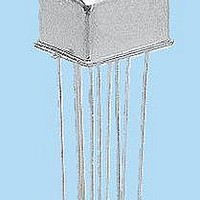
OUTLINE DIMENSIONS
Relay Series
Ground Pin Option
(See Appendix)
Pad Option
(See Appendix)
transfer in excess of 1 μsec.
estimates. No on-going verification tests are performed.
plated or solder coated leads.
on the relay.
Relay Series
Ground Pin Option
(See Appendix)
Pad Option
(See Appendix)
.017 (.43)
.335 MAX.
9 LEADS
(8.51)
+.002 (.051)
±.001 (.043)
.275 MAX.
.75 MIN.
(19.05)
DIA.
CASE DETAIL
(6.99)
DIMENSIONS ARE SHOWN IN INCHES (MILLIMETERS)
SPECIFICATIONS ARE SUBJECT TO CHANGE WITHOUT NOTICE
.435 MAX.
(11.05)
Teledyne Part Numbering System for
Teledyne Part Numbering System for Military Qualified (JAN) Relays
www.teledynerelays.com
ER 116C Z M9 - 26
J
(Viewed from Terminals; Numbers for Reference Only)
.031 ±.003
(.79 ±.08)
.100 ±.010
(2.54 ±.25)
116C
TYP
TERMINAL LOCATIONS
Z M9 - 26
7
6
9
8
.375 MAX.
(9.53)
10
1
2
3
4
(5.08 ±0.25)
® Established Reliability Relay
.200 ±.010
Notes:
Logic 1 activates the relay.
Logic 0 de-activates the relay.
Vcc = logic bias power.
Vr = coil energization voltage.
.475 MAX.
A / S Q
(12.06)
L
.035 ±.010
(.89 ±.25)
TYPICAL CMOS INTERFACE CIRCUIT
DC Logic Voltage Supply
1 = 3.8 to 15Vdc
0 = 0.5Vdc min.
Logic element
SCHEMATIC IS VIEWED FROM TERMINALS
SCHEMATIC DIAGRAM
Vcc
Screening and Reliability
Level
Coil Voltage
Q= Solder Coated Leads
G= Gold Plated Leads
(Notes 5 and 6)
S= 0.187" leads
(Note 6)
Screening and Reliability
Level
Coil Voltage
Pin10
Pin 1
Vr
PIN 1: + SUPPLY
PIN 9: – SUPPLY
PIN 10: GATE
Pin 9
116C Page 3
116C/1203/Q1
Related parts for J116CM9-5M
Image
Part Number
Description
Manufacturer
Datasheet
Request
R

Part Number:
Description:
RF (Radio Frequency) Relays DPDT 12VDC 0.1ohm w/M9 pad
Manufacturer:
TELEDYNE
Datasheet:

Part Number:
Description:
Relay; E-Mech; Freq (RF); DPDT; Cur-Rtg 1A; Ctrl-V 5DC; Vol-Rtg 28DC; PCB Mnt; 10 Pin
Manufacturer:
TELEDYNE
Datasheet:
Part Number:
Description:
Module; Thru Hole; Solid-State; 3.5 mA @ 115 V (RMS), 3.0 mA @ 220 V (RMS); 7
Manufacturer:
TELEDYNE
Datasheet:
Part Number:
Description:
Module; Thru Hole; Solid-State; 15 mA (Max.); 3.8 to 16 V (RMS); 3 VDC (Min.)
Manufacturer:
TELEDYNE
Datasheet: