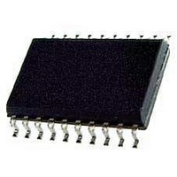
Si8502-C-IS Silicon Laboratories Inc, Si8502-C-IS Datasheet - Page 12

Si8502-C-IS
Manufacturer Part Number
Si8502-C-IS
Description
Board Mount Current Sensors 10A SNGLE OUTPUT 5kV
Manufacturer
Silicon Laboratories Inc
Type
AC Current Sensorr
Series
-r
Datasheet
1.SI8503-C-IS.pdf
(36 pages)
Specifications of Si8502-C-IS
Current Rating
10 A
Supply Voltage
2.7 V to 5.5 V
Frequency Range
50 KHz to 1 MHz
Operating Temperature
- 40 C to + 125 C
Accuracy
5 %
Current - Sensing
10A
Sensitivity
196mV/A
Current - Supply
4mA
Sensor Type
Closed Loop
Voltage - Supply
2.7 V ~ 5.5 V
Output
Configurable
Frequency
50kHz ~ 1MHz
Response Time
-
Polarization
Unidirectional
Package / Case
20-SOIC (0.295", 7.50mm Width)
Lead Free Status / RoHS Status
Lead free / RoHS Compliant
Si85xx
2.5. Effect of Temperature on Accuracy
Offset voltage present at the Si85xx output terminals
(output offset voltage) is calibrated out each time VDD is
applied to the Si85xx; so, its error contribution is
minimized when the temperature at which calibration
occurred is at or near the steady-state operating
temperature of the Si85xx. For example, applying VDD
at 25 °C (offset cal is performed) and operating at 85 °C
will result in a larger offset error than operating at 50 °C.
The effect of this error is summarized in Figure 6. The
chart is referenced to 25 °C. If the Si85xx is powered up
at 25 °C and then operated at 125 °C with no auto-
calibration performed (i.e., the power is not cycled at
125 °C, which causes an auto-calibration), a 3%
measurement error can be expected.
Figure 7 shows the Si85xx thermal characteristics of the
on-chip sense resistance over the temperature range of
–40 to +125 °C. Series inductance is constant at 2 nH
(max) across this same temperature range.
12
-0.5%
-1.0%
-1.5%
-2.0%
-2.5%
-3.0%
-3.5%
1.0%
0.5%
0.0%
1.8
1.6
1.4
1.2
0.8
0.6
0.4
0.2
Figure 7. Series Resistance Thermal
2
1
0
-20
Figure 6. Differential Temperature
0
0
25
Calibration Error
Characteristics
20
Temperature (Celcius)
Temperature (°C)
50
40
60
75
80
100
100
Preliminary Rev. 0.21
125
120
2.6. Leading Edge Noise Suppression
High-amplitude spikes on the leading edge of the
primary switching waveforms can cause the PWM latch
to be erroneously reset at the start of the switching cycle
when operating in current mode control. To prevent this
problem, leading edge blanking is commonly used to
disable the current comparator during the early portion
of the primary-side switching cycle. The Si85xx
eliminates leading-edge noise spikes by including them
in the signal integration. As shown in the output
waveform of Figure 8 (Si8502 waveform measured
directly on OUT pin with no external filter), noise present
in the input waveform is eliminated without the use of
blanking.
2.7. FAULT Output
The FAULT output (Si8517/8/9) guards against Si85xx
output signal errors caused by missing reset cycles.
FAULT is asserted when a measurement cycle exceeds
the internal watchdog timer times limit of t
can be used to alert a local microcontroller or digital
power controller of a current sense failure or to initiate a
system shutdown. To detect faults, tie a 200 k resistor
from TRST/FAULT to VDD.
2.8. Safe Operating Limits
The Si85xx is a very robust current sensor. Its maximum
input current rate of change is limited to 1000 A/µs. The
maximum peak ac input current limit is 200 A. The
thermal limit or continuous dc current flow limit is 30 A.
Exceeding these limits may cause long-term reliability
issues. Refer to “AN329: Extending the Full-Scale
Range of the Si85xx” for more information.
Figure 8. Leading-Edge Noise Suppression
Waveforms (200 kHz, 9.3 A Load)
Current Sense
Transformer
Si8502
WD
. FAULT


