TFS761HG Power Integrations, TFS761HG Datasheet - Page 13
TFS761HG
Manufacturer Part Number
TFS761HG
Description
Switching Converters, Regulators & Controllers 2 Swt Fwd,Flybk Cntr 326 W Cont. @ 25 C
Manufacturer
Power Integrations
Datasheet
1.TFS758HG.pdf
(36 pages)
Specifications of TFS761HG
Output Voltage
100 V to 400 V
Output Power
383 W
Switching Frequency
66 KHz
Operating Temperature Range
+ 150 C
Mounting Style
Through Hole
Duty Cycle (max)
73 %
Package / Case
eSIP-16B
Number Of Outputs
1
Lead Free Status / RoHS Status
Lead free / RoHS Compliant
Available stocks
Company
Part Number
Manufacturer
Quantity
Price
Company:

Part Number:
TFS761HG
Manufacturer:
POWER
Quantity:
15 000
Part Number:
TFS761HG
Manufacturer:
POWER
Quantity:
20 000


2. Second a 15 mA threshold (I
Note: unlike the TinySwitch-III the HiperTFS BYPASS pin capacitor
does not provide any programming capability. Instead the
recommended BYPASS pin capacitor should always be a 1 mF
(ceramic) capacitor.
Main and Standby Line Overvoltage Detection (OV)
The overvoltage threshold is included in the device, and can be
used to disable the device during overvoltage (with the use of
an additional external signal Zener). The overvoltage threshold
is set sufficiently high to prevent accidental triggering during
boost PFC overshoot conditions. When the overvoltage
condition is triggered, it will simultaneously shutdown both the
Main and Standby. The overvoltage feature is intended for use
with external components (circuitry), to program the overvoltage
threshold independently of the undervoltage thresholds (see the
Applications section for details).
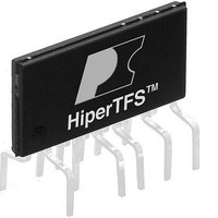
High-Power eSIP Package
The HiperTFS package is designed to minimize the physical size
of the device, while maintaining a low thermal impedance and
sufficient electrical spacing for the pins. The package has 12
functional pins with 4 pins removed for increased pin-to-pin
spacing between high-voltage pins. The low-side two-switch
forward and flyback MOSFETs have a thermal impedance of
less than 1 °C/W to the exposed pad on the back of the
package. Since this pad is referenced to the SOURCE pin
(Source), it is at electrical ground potential and thus can be
connected to the heat sink without need for electrical insulation.
The high-side MOSFET is over-molded to achieve electrical
isolation and thus also allows direct connection to the heat sink.
www.powerint.com
latch-off. When the BYPASS pin current exceeds this
threshold, the standby and main converters are latched-off.
This latch can be reset by pulling the LINE-SENSE pin below
the line undervoltage threshold (I
the BYPASS pin below 4.7 V.
BP(SD)
L(SB-UVOFF)
)for standby secondary OVP
), or by discharging
Output Power Table
Table 5.
TFS757HG
TFS758HG
TFS759HG
TFS760HG
TFS761HG
TFS762HG
TFS763HG
TFS764HG
Notes:
1. Maximum practical continuous power in an open frame design with adequate
2. Package: eSIP16/12. (Note: Direct attach to heat sink, does not require
heat sinking (assuming heat sink θ
ambient temperature (see Key Applications Considerations for more information).
insulation SIL pad)
Product
Output Power Table.
2
Continuous
193 W
236 W
280 W
305 W
326 W
360 W
388 W
414 W
(25 °C)
Two-Switched Forward
1
C-A
Continuous
of <4 °C/W), measured at specified
163 W
200 W
235 W
258 W
276 W
304 W
327 W
344 W
(50 °C)
380 V
TFS757-764HG
1
228 W
278 W
309 W
358 W
383 W
407 W
455 W
530 W
(50 °C)
Peak
100 V - 400 V
Flyback
Rev. C 02/11
50 °C
20 W
20 W
20 W
20 W
20 W
20 W
20 W
20 W
13
Related parts for TFS761HG
Image
Part Number
Description
Manufacturer
Datasheet
Request
R

Part Number:
Description:
SOP-16
Manufacturer:
Power Integrations
Datasheet:
Part Number:
Description:
DIP8
Manufacturer:
Power Integrations
Datasheet:
Part Number:
Description:
TO-263
Manufacturer:
Power Integrations
Datasheet:
Part Number:
Description:
TO-263
Manufacturer:
Power Integrations
Datasheet:
Part Number:
Description:
Manufacturer:
Power Integrations
Datasheet: