Rev 2.0 ©2010 Advanced Linear Devices, Inc. 415 Tasman Drive, Sunnyvale, CA 94089-1706 Tel: (408) 747-1155 Fax: (408) 747-1286
GENERAL DESCRIPTION
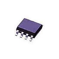
The ALD555 timer is a high performance monolithic timing circuit built
with advanced silicon gate CMOS technology. It offers the benefits of
high input impedance, thereby allowing smaller timing capacitors and
longer timing cycle; high speed, with typical cycle time of 500ns; low
power dissipation for battery operated environment; reduced supply
current spikes, allowing smaller and lower cost decoupling capacitors.
It is capable of producing accurate time delays and oscillations in both
monostable and astable operation. It operates in the one-shot (mono-
stable) mode or 50% duty cycle free running oscillation mode with a
single resistor and one capacitor. The inputs and outputs are fully
compatible with CMOS, NMOS or TTL logic.
There are three matched internal resistors (approximately 200KΩ
each) that set the threshold and trigger levels at two-thirds and one-
third respectively of V +
control terminal (pin 5). When the trigger input is below the trigger level,
the output is in the high state and sourcing 2mA. When threshold input
is above the threshold level at the same time the trigger input is above
the trigger level, the internal flip-flop is reset, the output goes to the low
state and sinks up to 10mA. The reset input overrides all other inputs
and when it is active (reset voltage less than 1V), the output is in the
low state.
FEATURES
• Functional equivalent to NE555 with greatly expanded high
• High speed, low power, monolithic CMOS technology
• Low supply current: 100
• Extremely low trigger, threshold and reset currents:1pA typical
• High speed operation -- 2MHz oscillation
• Low operating supply voltage of 2 to 12V
• Operates in both monostable and astable modes
• Fixed 50% duty cycle or adjustable duty cycle
• CMOS, NMOS and TTL compatible input/output
• High discharge sinking current of 80mA
• Low supply current spikes
* Contact factory for leaded (non-RoHS) or high temperature versions.
ORDERING INFORMATION (“L” suffix denotes lead-free (RoHS))
0°C to +70°C
8-Pin Small Outline
Package (SOIC)
ALD555SAL
and low frequency ranges
A
L
D
INEAR
DVANCED
EVICES,
Operating Temperature Range *
.
I
NC.
These levels can be adjusted by using the
µ
A typical
0°C to +70°C
8-Pin Plastic
DIP Package
ALD555PAL
HIGH SPEED CMOS TIMER
-55°C to +125°C
8-Pin CERDIP
Package
ALD555DA
www.aldinc.com
APPLICATIONS
PIN CONFIGURATION
BLOCK DIAGRAM
•
• Precision timing
• Sequential timing
• Long delay timer
• Pulse width and pulse position
• Missing pulse detector
• Frequency divider
THRESHOLD
CONTROL
TRIGGER
High speed one-shot (monostable)
pulse generation
modulation
GROUND
TRIGGER
OUTPUT
(6)
(5)
(2)
RESET
GND
(1)
R
R
R
4
2
1
3
SAL, PAL, DA PACKAGES
V
(8)
+
R
S
RESET
(4)
8
5
7
6
DISCHARGE
V
THRESHOLD
CONTROL
+
ALD555
OUTPUT
DISCHARGE
(3)
(7)


