MC56F8257VLH Freescale Semiconductor, MC56F8257VLH Datasheet - Page 74
MC56F8257VLH
Manufacturer Part Number
MC56F8257VLH
Description
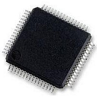
DSC 64K FLASH 60MHZ 64-LQFP
Manufacturer
Freescale Semiconductor
Series
56F8xxxr
Datasheets
1.TWR-56F8257.pdf
(88 pages)
2.MC56F8245VLD.pdf
(14 pages)
3.MC56F8245VLD.pdf
(2 pages)
4.MC56F8245VLD.pdf
(629 pages)
Specifications of MC56F8257VLH
Core Processor
56800E
Core Size
16-Bit
Speed
60MHz
Connectivity
CAN, I²C, LIN, SCI, SPI
Peripherals
LVD, POR, PWM, WDT
Number Of I /o
54
Program Memory Size
64KB (32K x 16)
Program Memory Type
FLASH
Ram Size
4K x 16
Voltage - Supply (vcc/vdd)
3 V ~ 3.6 V
Data Converters
A/D 16x12b, D/A 1x12b
Oscillator Type
Internal
Operating Temperature
-40°C ~ 105°C
Package / Case
64-LQFP
Product
DSCs
Processor Series
56800E
Core
56800E
Device Million Instructions Per Second
60 MIPs
Maximum Clock Frequency
60 MHz
Number Of Programmable I/os
54
Data Ram Size
8 KB
Operating Supply Voltage
3.3 V
Maximum Operating Temperature
+ 105 C
Mounting Style
SMD/SMT
Minimum Operating Temperature
- 40 C
On-chip Adc
12 bit, 8 Channel
Package
64LQFP
Family Name
MC56F82xx
Maximum Speed
60 MHz
Data Bus Width
16 Bit
Interface Type
CAN/I2C/SCI/SPI
On-chip Dac
1-chx12-bit
Number Of Timers
8
Lead Free Status / RoHS Status
Lead free / RoHS Compliant
Eeprom Size
-
Lead Free Status / Rohs Status
Details
Available stocks
Company
Part Number
Manufacturer
Quantity
Price

Company:
Part Number:
MC56F8257VLH
Manufacturer:
Freescale Semiconductor
Quantity:
10 000
Part Number:
MC56F8257VLH
Manufacturer:
FREESCALE
Quantity:
20 000


Ordering Information
Use the following list of considerations to assure correct operation of the MC56F825x/MC56F824x:
9
Table 46
distributor to determine availability and to order devices.
74
•
•
•
•
•
•
•
•
•
•
•
•
•
•
•
•
Provide a low-impedance path from the board power supply to each V
from the board ground to each V
The minimum bypass requirement is to place 0.01–0.1 µF capacitors positioned as near as possible to the package
supply pins. The recommended bypass configuration is to place one bypass capacitor on each of the V
including V
Ensure that capacitor leads and associated printed circuit traces that connect to the chip V
as short as possible.
Bypass the V
PCB trace lengths should be minimal for high-frequency signals.
Consider all device loads as well as parasitic capacitance due to PCB traces when calculating capacitance. This is
especially critical in systems with higher capacitive loads that could create higher transient currents in the V
V
Take special care to minimize noise levels on the V
Using separate power planes for V
Connect the separate analog and digital power and ground planes as near as possible to power supply outputs. If an
analog circuit and digital circuit are powered by the same power supply, you should connect a small inductor or ferrite
bead in serial with V
Physically separate analog components from noisy digital components by ground planes. Do not place an analog trace
in parallel with digital traces. Place an analog ground trace around an analog signal trace to isolate it from digital traces.
Because the flash memory is programmed through the JTAG/EOnCE port, SPI, SCI, or I
provide an interface to this port if in-circuit flash programming is desired.
If desired, connect an external RC circuit to the RESET pin. The resistor value should be in the range of 4.7 k to
10 k ; the capacitor value should be in the range of 0.22 µF to 4.7 µF.
Configuring the RESET pin to GPIO output in normal operation in a high-noise environment may help to improve the
performance of noise transient immunity.
Add a 2.2 k external pullup on the TMS pin of the JTAG port to keep EOnCE in a restate during normal operation if
a JTAG converter is not present.
During reset and after reset but before I/O initialization, all I/O pins are at input state with internal pullup enabled. The
typical value of internal pullup is around 110 k . These internal pullups can be disabled by software.
To eliminate PCB trace impedance effect, each ADC input should have an RC filter of no less than 33 pF 10 .
External clamp diodes on analog input pins are recommended.
lists the pertinent information needed to place an order. Consult a Freescale Semiconductor sales office or authorized
SS
Ordering Information
circuits.
DDA
DD
/V
and V
SSA.
DDA
SS
Ceramic and tantalum capacitors tend to provide better tolerances.
MC56F825x/MC56F824x Digital Signal Controller, Rev. 3
and V
with approximately 100 µF, plus the number of 0.1 µF ceramic capacitors.
SSA
SS
DD
(GND) pin.
traces.
and V
DDA
and separate ground planes for V
REF
, V
DDA
, and V
SSA
DD
pin on the MC56F825x/MC56F824x and
pins.
SS
and V
2
DD
C, the designer should
SSA
Freescale Semiconductor
and V
is recommended.
SS
(GND) pins are
DD
/V
SS
DD
pairs,
and
Related parts for MC56F8257VLH
Image
Part Number
Description
Manufacturer
Datasheet
Request
R

Part Number:
Description:
Manufacturer:
Freescale Semiconductor, Inc
Datasheet:
Part Number:
Description:
Manufacturer:
Freescale Semiconductor, Inc
Datasheet:
Part Number:
Description:
Manufacturer:
Freescale Semiconductor, Inc
Datasheet:
Part Number:
Description:
Manufacturer:
Freescale Semiconductor, Inc
Datasheet:
Part Number:
Description:
Manufacturer:
Freescale Semiconductor, Inc
Datasheet:
Part Number:
Description:
Manufacturer:
Freescale Semiconductor, Inc
Datasheet:
Part Number:
Description:
Manufacturer:
Freescale Semiconductor, Inc
Datasheet:
Part Number:
Description:
Manufacturer:
Freescale Semiconductor, Inc
Datasheet:
Part Number:
Description:
Manufacturer:
Freescale Semiconductor, Inc
Datasheet:
Part Number:
Description:
Manufacturer:
Freescale Semiconductor, Inc
Datasheet:
Part Number:
Description:
Manufacturer:
Freescale Semiconductor, Inc
Datasheet:
Part Number:
Description:
Manufacturer:
Freescale Semiconductor, Inc
Datasheet:
Part Number:
Description:
Manufacturer:
Freescale Semiconductor, Inc
Datasheet:
Part Number:
Description:
Manufacturer:
Freescale Semiconductor, Inc
Datasheet:
Part Number:
Description:
Manufacturer:
Freescale Semiconductor, Inc
Datasheet: