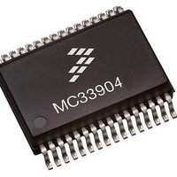
MCZ33904B3EK Freescale Semiconductor, MCZ33904B3EK Datasheet - Page 63

MCZ33904B3EK
Manufacturer Part Number
MCZ33904B3EK
Description
IC SBC CAN HS 3.3V 32SOIC
Manufacturer
Freescale Semiconductor
Type
High Speed CAN Interfacer
Specifications of MCZ33904B3EK
Operating Supply Voltage
3.3 V
Supply Current
2 mA
Package / Case
SOIC-32
Mounting Style
SMD/SMT
Product
CAN
Lead Free Status / RoHS Status
Lead free / RoHS Compliant
Available stocks
Company
Part Number
Manufacturer
Quantity
Price
Company:
Part Number:
MCZ33904B3EKR2
Manufacturer:
FREESCA
Quantity:
4 975
INIT REGISTERS
Analog Integrated Circuit Device Data
Freescale Semiconductor
Table 15. Initialization Regulator Registers, INIT REG (note: register can be written only in INIT mode)
Note: these registers can be written only in INIT mode
[b_15 b_14] 0_0101 [P/N]
b6, b5
b4, b3
b1, b0
MOSI First Byte [15-8]
Bit
Condition for default
b7
00
01
10
11
00
01
10
11
b2
00
01
10
11
0
1
0
1
01 00 _ 101 P
Default state
V
DD RST
D[1] V
I/O-x sync
Cyclic on[1] Cyclic on[0] - Determine I/O-0 activation time, when cyclic sense function is selected
I/O-x sync - Determine if I/O-1 is sensed during I/O-0 activation, when cyclic sense function is selected
V
bit 7
DD RST
DDL RST
1
D[0] - Select the RESET pin low lev duration, after V
[1] V
V
DDL RST
DDL
bit 6
1600 μs (typical value. ref to dynamic parameters for exact value)
0
200 μs (typical value. ref to dynamic parameters for exact value)
400 μs (typical value. ref to dynamic parameters for exact value)
800 μs (typical value. ref to dynamic parameters for exact value)
rst[1]
[0] - Select the V
INT at approx 0.9 V
V
[V
DDL
AUX
bit 5
0
I/O-1 sense during I/O-0 activation
rst[0]
5/3] - Select Vauxilary output voltage
Reset at approx 0.9 V
Reset at approx 0.9 V
Reset at approx 0.7 V
DD
I/O-1 sense anytime
under-voltage threshold, to activate RESET pin and/or INT
V
Description
V
V
MOSI Second Byte, bits 7-0
DD
AUX
AUX
DD
bit 4
1.0 ms
5.0 ms
10 ms
20 ms
rstD[1]
0
, Reset at approx 0.7 V
= 3.3 V
= 5.0 V
POR
DETAIL OF CONTROL BITS AND REGISTER MAPPING
V
DD
DD
DD
DD
bit 3
.
.
DD
rstD[0]
0
rises above the V
DD
V
AUX
bit 2
0
SERIAL PERIPHERAL INTERFACE
5/3
DD
under-voltage threshold
Cyclic on[1]
bit 1
0
Cyclic on[0]
bit 0
33903/4/5
0
63


