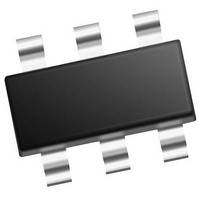
MCP65R41T-2402E/CHY Microchip Technology, MCP65R41T-2402E/CHY Datasheet - Page 24

MCP65R41T-2402E/CHY
Manufacturer Part Number
MCP65R41T-2402E/CHY
Description
IC COMPARATOR 2.4V REF SOT-23-6
Manufacturer
Microchip Technology
Type
General Purposer
Datasheet
1.MCP65R41T-1202ECHY.pdf
(34 pages)
Specifications of MCP65R41T-2402E/CHY
Output Type
CMOS, Push-Pull, TTL
Package / Case
*
Number Of Elements
1
Voltage - Supply
1.8 V ~ 5.5 V
Mounting Type
Surface Mount
Product
Digital Comparators
Offset Voltage (max)
10 mV
Input Bias Current (max)
1 pA
Supply Voltage (max)
5.5 V
Supply Voltage (min)
1.8 V
Maximum Operating Temperature
+ 125 C
Mounting Style
SMD/SMT
High Level Output Current
- 100 nA
Minimum Operating Temperature
- 40 C
Comparator Type
Low Power
No. Of Comparators
1
Ic Output Type
Push Pull
Output Compatibility
CMOS, TTL
Supply Current
2.5µA
Supply Voltage Range
1.8V To 5.5V
Amplifier Case Style
SOT-23
Rohs Compliant
No
Lead Free Status / RoHS Status
Lead free / RoHS Compliant
Other names
MCP65R41T-2402E/CHY
MCP65R41T-2402E/CHYTR
MCP65R41T-2402E/CHYTR
Available stocks
Company
Part Number
Manufacturer
Quantity
Price
Company:
Part Number:
MCP65R41T-2402E/CHY
Manufacturer:
RENESAS
Quantity:
694
Company:
Part Number:
MCP65R41T-2402E/CHY
Manufacturer:
Microchip Technology
Quantity:
135
MCP65R41/6
4.6
In applications where the low input bias current is
critical, the Printed Circuit Board (PCB) surface
leakage effects need to be considered. Surface
leakage is caused by humidity, dust or other type of
contamination on the board. Under low humidity
conditions, a typical resistance between nearby traces
is 10
to flow. This is greater than the MCP65R41/6 family’s
bias current at +25°C (1 pA, typical).
The easiest way to reduce the surface leakage is to use
a guard ring around the sensitive pins (or traces). The
guard ring is biased at the same voltage as the
sensitive pin. An example of this type of layout is shown
in
FIGURE 4-9:
for Inverting Circuit.
1.
2.
4.7
4.7.1
Some applications require a higher DC precision. An
easy way to solve this problem is to use an amplifier
(such as the MCP6041, a 600 nA low power and
14 kHz bandwidth op amp) to gain-up the input signal
before it reaches the comparator.
an example of this approach, which also level shifts to
V
DS22269A-page 24
PU
Inverting Configuration
a)
b)
Non-inverting Configuration
a)
b)
using the Open-Drain option, MCP65R46.
12
Figure
. A 5V difference would cause 5 pA of current
PCB Surface Leakage
Connect the guard ring to the non-inverting
input pin (V
to the same reference voltage as the
comparator (e.g., V
Connect the inverting pin (V
pad without touching the guard ring.
Connect the non-inverting pin (V
input pad without touching the guard ring.
Connect the guard ring to the inverting input
pin (V
Typical Applications
PRECISE COMPARATOR
4-9.
IN
–).
IN-
IN
Guard Ring
+). This biases the guard ring
Example Guard Ring Layout
(Figures 4-6
DD
/2 or ground).
IN+
(Figure
Figure 4-10
IN
–) to the input
4-4):
and 4-9):
IN
V
+) to the
SS
shows
FIGURE 4-10:
Comparator.
4.7.2
A simple bistable multi-vibrator design is shown in
Figure
maximum comparator internal V
oscillation. The output duty cycle changes with V
FIGURE 4-11:
4.7.3
The MCP65R41 device can be used as an over
temperature protection circuit using a thermistor. The
2.4V V
thermistor, the alert threshold and hysteresis threshold.
This is ideal for battery powered applications, where
the change in temperature and output toggle
thresholds would remain fixed as battery voltage
decays over time.
FIGURE 4-12:
Circuit.
V
Thermistor
V
IN
REF
V
REF
REF
4-11. V
R
4
V
R
REF
1
can be used as stable reference to the
BISTABLE MULTI-VIBRATOR
OVER TEMPERATURE
PROTECTION CIRCUIT
R
R
REF
2
3
R
V
MCP6041
REF
1
C
needs to be between ground and the
1
R
V
* Pull-up resistor required for the
MCP65R46 only.
2
V
Precise Inverting
Bistable Multi-Vibrator.
Over Temperature Alert
DD
V
REF
2010 Microchip Technology Inc.
REF
V
MCP65R41
DD
R
V
F
REF
REF
V
R
R
PU
2
3
V
R
of 2.4V to achieve
DD
PU
V
DD
*
V
MCP65R46
OUT
V
PU
V
R
OUT
PU
V
REF
OUT
.


