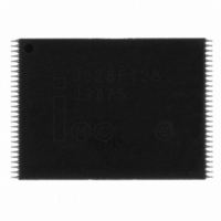
JS28F128J3D75A NUMONYX, JS28F128J3D75A Datasheet - Page 33

JS28F128J3D75A
Manufacturer Part Number
JS28F128J3D75A
Description
IC FLASH 128MBIT 75NS 56TSOP
Manufacturer
NUMONYX
Datasheet
1.JS28F128J3D75A.pdf
(68 pages)
Specifications of JS28F128J3D75A
Format - Memory
FLASH
Memory Type
FLASH
Memory Size
128M (16Mx8, 8Mx16)
Speed
75ns
Interface
Parallel
Voltage - Supply
2.7 V ~ 3.6 V
Operating Temperature
-40°C ~ 85°C
Package / Case
56-TSOP
Lead Free Status / RoHS Status
Lead free / RoHS Compliant
Other names
872766
872766
JS28F128J3D75
JS28F128J3D75 872766
872766
JS28F128J3D75
JS28F128J3D75 872766
Available stocks
Company
Part Number
Manufacturer
Quantity
Price
Part Number:
JS28F128J3D75A
Manufacturer:
INTEL/英特尔
Quantity:
20 000
Numonyx™ Embedded Flash Memory (J3 v. D)
Note:
Table 16: Enhanced Configuration Register
Table 17: Asynchronous 8-Word Page Mode Command Bus-Cycle Definition
8.1.2
8.2
November 2007
308551-05
Set Enhanced Configuration
Register (Set ECR)
ECR
ECR[15:14]
15
Reserved
ECR[12:0]
1. X = Any valid address within the device. ECD = Enhanced Configuration Register Data
ECR[13]
BITS
ECR
Command
14
RFU
RFU
Length
For forward compatibility reasons, if the 8-word Asynchronous Page mode is used on
Numonyx™ Embedded Flash Memory (J3 v. D), a Clear Status Register command must
be executed after issuing the Set Enhanced Configuration Register command. See
Table 17
• “1” = 8 Word Page mode
• “0” = 4 Word Page mode
Output Disable
With CEx asserted, and OE# at a logic-high level (V
Output signals D[15:0] are placed in a high-impedance state.
Bus Writes
Writing or Programming to the device, is where the host writes information or data into
the flash device for non-volatile storage. When the flash device is programmed, ‘ones’
are changed to ‘zeros’. ‘Zeros’ cannot be programed back to ‘ones’. To do so, an erase
operation must be performed. Writing commands to the Command User Interface (CUI)
enables various modes of operation, including the following:
Erasing is performed on a block basis – all flash cells within a block are erased together.
Any information or data previously stored in the block will be lost. Erasing is typically
done prior to programming. The Block Erase command requires appropriate command
data and an address within the block to be erased. The Byte/Word Program command
requires the command and address of the location to be written. Set Block Lock-Bit
commands require the command and block within the device to be locked. The Clear
Block Lock-Bits command requires the command and address within the device to be
cleared.
Page
ECR
• Reading of array data
• Common Flash Interface (CFI) data
• Identifier codes, inspection, and clearing of the Status Register
• Block Erasure, Program, and Lock-bit Configuration (when V
13
ECR
for further details.
12
Required
Cycles
Bus
ECR
2
11
DESCRIPTION
ECR
10
Oper
Write
ECR
9
First Bus Cycle
ECR
Addr
8
ECD
(1)
ECR
7
Reserved
ECR
0060h
Data
6
All bits should be set to 0.
All bits should be set to 0.
IH
ECR
5
), the device outputs are disabled.
Oper
Write
ECR
4
Second Bus Cycle
ECR
PEN
3
NOTES
Addr
= V
ECD
ECR
2
(1)
PENH
ECR
)
1
Datasheet
0004h
Data
ECR
0
33


