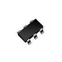
NCP1251ASN65T1G ON Semiconductor, NCP1251ASN65T1G Datasheet - Page 4

NCP1251ASN65T1G
Manufacturer Part Number
NCP1251ASN65T1G
Description
IC PWM CTLR OCP LATCH OVP 6TSOP
Manufacturer
ON Semiconductor
Datasheet
1.NCP1251ASN65T1G.pdf
(22 pages)
Specifications of NCP1251ASN65T1G
Output Isolation
Isolated
Frequency Range
61kHz ~ 71kHz
Voltage - Input
9.4 V ~ 28 V
Voltage - Output
12V
Operating Temperature
-40°C ~ 125°C
Package / Case
6-TSOP (0.063", 1.60mm Width)
Number Of Outputs
1
Duty Cycle (max)
84 %
Output Current
300 mA
Mounting Style
SMD/SMT
Switching Frequency
65 KHz
Operating Supply Voltage
28 V
Supply Current
2.1 mA
Maximum Operating Temperature
+ 125 C
Fall Time
30 ns
Minimum Operating Temperature
- 40 C
Rise Time
40 ns
Lead Free Status / RoHS Status
Lead free / RoHS Compliant
Available stocks
Company
Part Number
Manufacturer
Quantity
Price
Company:
Part Number:
NCP1251ASN65T1G
Manufacturer:
ON Semiconductor
Quantity:
155
Part Number:
NCP1251ASN65T1G
Manufacturer:
ON/安森美
Quantity:
20 000
Stresses exceeding Maximum Ratings may damage the device. Maximum Ratings are stress ratings only. Functional operation above the
Recommended Operating Conditions is not implied. Extended exposure to stresses above the Recommended Operating Conditions may affect
device reliability.
1. This device series contains ESD protection and exceeds the following tests: Human Body Model 2000 V per Mil−Std−883, Method 3015.
2. This device contains latch−up protection and exceeds 100 mA per JEDEC Standard JESD78.
MAXIMUM RATINGS TABLE
ELECTRICAL CHARACTERISTICS
(For typical values T
SUPPLY SECTION
DRIVE OUTPUT
CURRENT COMPARATOR
3. Guaranteed by design
4. See characterization table for linearity over negative bias voltage
5. A 1 MW resistor is connected from pin 3 to the ground for the measurement.
VCC
ICC
VCC
V
Symbol
Symbol
ICCstby
V
V
VCC
T
Machine Model Method 200 V.
V
V
I
DRVhigh
IOPP
ICC1
ICC2
ICC3
ICC2
ICC3
source
DRVlow
R
ZENER
R
V
R
I
J,max
Limit1
Limit2
sink
I
LATCH
T
T
qJA
CC
OH
IB
OL
HYST
(min)
r
f
ON
Power Supply voltage, V
Maximum voltage on low power pins CS, FB and OPP
Maximum injected negative current into the OPP pin (pin 1)
Thermal Resistance Junction−to−Air
Maximum Junction Temperature
Storage Temperature Range
ESD Capability, Human Body Model (HBM), all pins
ESD Capability, Machine Model (MM)
V
V
Hysteresis VCC
Clamped V
Start−up current
Internal IC consumption with I
Internal IC consumption with I
Internal IC consumption with I
Internal IC consumption with I
Current flowing into V
Internal IC consumption while in skip cycle (V
MOSFET)
Output voltage rise−time @ C
Output voltage fall−time @ C
Source resistance
Sink resistance
Peak source current, V
Peak sink current, V
DRV pin level at V
DRV pin level at V
Input Bias Current @ 0.8 V input level on pin 4
Maximum internal current setpoint – T
Maximum internal current setpoint – T
CC
CC
increasing level at which driving pulses are authorized
decreasing level at which driving pulses are stopped
J
= 25°C, for min/max values T
CC
when latched off / burst mode activation @ I
ON
CC
CC
− VCC
GS
CC
close to VCC
= 28 V – DRV unloaded
GS
= 12 V – (Note 3)
CC
pin that keeps the controller latched
(min)
= 0 V – (Note 3)
pin, continuous voltage
L
FB
FB
FB
FB
L
= 1 nF, 10−90% of output signal
= 1 nF, 10−90% of output signal
= 50 mA, F
= 50 mA, F
= 50 mA, F
= 50 mA, F
(min)
J
Rating
J
J
= −40°C to +125°C, Max T
= 25°C – pin1 grounded
= −40°C to 125°C – pin 3 grounded
with a 33 kW resistor to GND
Rating
SW
SW
SW
SW
http://onsemi.com
CC
= 65 kHz and C
= 65 kHz and C
= 100 kHz and C
= 100 kHz and C
= 12 V, driving a typical 6 A/600 V
4
CC
= 500 mA
L
L
L
L
= 0 nF
= 1 nF
J
= 0 nF
= 1 nF
= 150°C, V
CC
= 12 V unless otherwise noted)
Pin
5
5
5
5
5
5
5
5
5
5
5
6
6
6
6
6
6
6
6
4
4
4
0.744
0.72
Min
−60 to +150
8.2
16
30
10
−0.3 to 10
6
−
−
−
−
−
−
−
−
−
−
8
Value
360
150
200
28
−2
2
0.02
Typ
550
300
500
8.8
1.4
2.1
1.7
3.1
6.0
0.8
0.8
18
40
30
13
12
−
7
−
−
0.856
Max
0.88
9.4
2.2
3.0
2.5
4.0
20
15
14
−
−
−
−
−
−
−
°C/W
Unit
mA
kV
°C
°C
V
V
V
Unit
mA
mA
mA
mA
mA
mA
mA
mA
mA
mA
ns
ns
V
V
V
V
W
W
V
V
V
V


