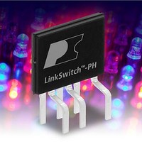
LNK419EG Power Integrations, LNK419EG Datasheet - Page 11

LNK419EG
Manufacturer Part Number
LNK419EG
Description
IC LED DRIVER 50W ESIP-7C
Manufacturer
Power Integrations
Series
LinkSwitch®-PHr
Type
Off Line Switcherr
Datasheet
1.LNK403EG.pdf
(20 pages)
Specifications of LNK419EG
Constant Current
Yes
Internal Driver
Yes
Type - Primary
General Purpose
Type - Secondary
White LED
Mounting Type
Through Hole
Topology
AC DC Offline Switcher, PWM
Number Of Outputs
1
Frequency
62kHz ~ 70kHz
Package / Case
7-SIP, 6 Leads, Exposed Pad, Formed Leads
Operating Temperature
-20°C ~ 125°C
Output Voltage
85 VAC to 308 VAC
Input / Supply Voltage (max)
308 VAC
Input / Supply Voltage (min)
85 VAC
Duty Cycle (max)
99.9 %
Switching Frequency
66 KHz
Supply Current
1.5 mA
Operating Temperature Range
- 40 C to + 150 C
Mounting Style
Through Hole
Output Current
0.5 A
Output Power
50 W
Lead Free Status / RoHS Status
Lead free / RoHS Compliant
Voltage - Supply
-
Voltage - Output
-
Other names
596-1397
Available stocks
Company
Part Number
Manufacturer
Quantity
Price
Company:
Part Number:
LNK419EG
Manufacturer:
TEAC
Quantity:
201
Part Number:
LNK419EG
Manufacturer:
POWER
Quantity:
20 000
Layout Considerations
Primary Side Connections
Use a single point (Kelvin) connection at the negative terminal of
the input filter capacitor for the SOURCE pin and bias returns.
This improves surge capabilities by returning surge currents
from the bias winding directly to the input filter capacitor. The
BYPASS pin capacitor should be located as close to the
BYPASS pin and connected as close to the SOURCE pin as
possible. The SOURCE pin trace should not be shared with the
main power MOSFET switching currents. All FEEDBACK pin
Figure 11. RD-193 7 W Layout Example, Top Layer.
www.powerint.com
N
L
RV1
F1
Input EMI Filter
Copper Area for
L1
Heat Sinking
L2
R3
C2
R2
R16
R14
Bulk Capacitor
C9
L3
R24
C14
VR3
components that connect to the SOURCE pin should follow the
same rules as the BYPASS pin capacitor. It is critical that the
main power MOSFET switching currents return to the bulk
capacitor with the shortest path as possible. Long high current
paths create excessive conducted and radiated noise.
Secondary Side Connections
The output rectifier and output filter capacitor should be as
close as possible. The transformer’s output return pin should
have a short trace to the return side of the output filter capacitor.
C3
VR1
C8
Clamp
D8
R10
D1
FL1
U1
C6
C12
BYPASS Pin
LNK403EG
Capacitor
T1
C7
2
LNK403-409EG/413-419EG
1
C5
Transformer
6
V
3
4
C4
5
V
Capacitors
Output
Filter
PI-5987-060110
Rev. B 11/10
11


