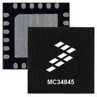
MC34845DEPR2 Freescale Semiconductor, MC34845DEPR2 Datasheet - Page 8

MC34845DEPR2
Manufacturer Part Number
MC34845DEPR2
Description
IC LED DVR BACKLIGHT 6CH 24QFN
Manufacturer
Freescale Semiconductor
Datasheet
1.MC34845AEP.pdf
(20 pages)
Specifications of MC34845DEPR2
Internal Driver
Yes
Type - Primary
Backlight
Mounting Type
Surface Mount
Topology
PWM, Step-Up (Boost)
Number Of Outputs
6
Frequency
270kHz ~ 330kHz
Voltage - Supply
5 V ~ 21 V
Voltage - Output
60V
Package / Case
24-UFQFN Exposed Pad
Operating Temperature
-40°C ~ 85°C
Operating Supply Voltage
5 V to 21 V
Maximum Supply Current
5 mA
Maximum Power Dissipation
3.4 W
Maximum Operating Temperature
+ 85 C
Mounting Style
SMD/SMT
Minimum Operating Temperature
- 40 C
Lead Free Status / RoHS Status
Lead free / RoHS Compliant
Table 4. 34845 Pin Definitions
Pin Number
13, 19, 21
PIN CONNECTIONS
STATIC AND DYNAMIC ELECTRICAL CHARACTERISTICS
8
34845
7 - 12
EP
14
15
16
17
18
20
22
23
24
1
2
3
4
5
6
TRANSPARENT
TOP VIEW
CH1 - CH6
Pin Name
PGNDB
PGNDA
COMP
WAKE
VDC1
VDC2
VOUT
PWM
SWB
SWA
GND
ISET
FAIL
OVP
VIN
EN
EP
Main voltage supply Input. IC Power input supply voltage, is used internally to produce internal voltage regulation
for logic functioning, and also as an input voltage for the boost regulator.
Power ground. This is the ground terminal for the internal Boost FET.
Boost switch node connection B. Switching node of boost converter.
Boost switch node connection A. Switching node of boost converter.
Power ground. This is the ground terminal for the internal Boost FET.
Enable pin (active high, internal pull-down).
LED string connections 1 to 6. LED current drivers. Each line has the capability of driving up to 30 mA.
Ground Reference for all internal circuits other than the Boost FET. The Exposed Pad (EP) should be used for
thermal heat dissipation.
Fault detected pin (open drain):
When a fault situation is detected, this pin goes into high impedance.
LED current setting. The maximum current is set using a resistor from this pin to GND.
External PWM control signal.
Boost compensation component connection. This passive terminal is used to compensate the boost converter.
Add a capacitor and a resistor in series to GND to stabilize the system as well as a shunt capacitor.
Low power consumption mode for single wire control. This is achieved by connecting the WAKE and PWM pins
together and grounding the ENABLE (EN) pin.
2.5 V internal voltage decoupling. This pin is for internal use only, and not to be used for other purposes. A
capacitor of 2.2 μF should be connected between this pin and ground.
External boost over-voltage setting. Requires a resistor divider from VOUT to GND. If no external OVP setting
is desired, this pin should be grounded.
6.0 V internal voltage decoupling. This pin is for internal use only, and not to be used for other purposes. A
capacitor of 2.2 μF should be connected between this pin and ground.
Boost voltage output feedback.
Ground and thermal enhancement pad
No Failure = Low-impedance pull-down
Failure = High-impedance
PGNDB
PGNDA
SWB
SWA
VIN
EN
1
2
3
4
5
6
Figure 3. 34845 Pin Connections
PIN CONNECTIONS
24
7
23
8
22
EP GND
9
21
10
20
11
Definition
19
12
18
17
16
15
14
13
WAKE
COMP
PWM
ISET
FAIL
GND
Analog Integrated Circuit Device Data
Freescale Semiconductor


