MC13892VK Freescale Semiconductor, MC13892VK Datasheet
MC13892VK
Specifications of MC13892VK
Available stocks


Related parts for MC13892VK

MC13892VK Summary of contents
Page 1
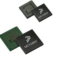
... The package style is a low profile BGA semi populated matrix, MC13892VK includes 139 balls including 4 sets of triple corner balls total 131 assigned signal pins, where the MC13892VL includes 186 balls, all of which are assigned signal pins. © ...
Page 2
... PACKAGING 13892 2 Figure 1. MC13892JVK Package Analog Integrated Circuit Device Data Freescale Semiconductor ...
Page 3
... Analog Integrated Circuit Device Data Freescale Semiconductor Figure 2. MC13892JVL Package PACKAGING 13892 3 ...
Page 4
... The MC13892JVK footprint consists of 10 mil pads with a 19.68 mil pitch, and the MC13892JVL footprint has 16 mil pads with a 31.496mil pitch. These are recommended as shown in Figure 3. Recommended Footprint for the MC13892JVK (Top View) Figure 4. Recommended Footprint for the MC13892JVL (Top View) 13892 4 Figures 3 through 4. Analog Integrated Circuit Device Data Freescale Semiconductor ...
Page 5
... SPIVC C PW GTDRV1 L GNDSW EN3 GEN2 VSRTC GND RTC N VG EN3 VGEN 3 VIN GEN3D RV VGE N2DR V Analog Integrated Circuit Device Data Freescale Semiconductor GN DBL ORE LED B LED KP LEDR GND CORE VCOREDIG LEDMD DV S1 REFC ORE CHR GSE1B LIC ELL B ATTFE T UID ...
Page 6
... SW1IN SW2FB SW2IN SW2IN VVIDEODRV GNDSW2 GNDSW2 TSY2 STANDBYSEC VVIDEO SW2OUT VGEN1 TSX1 TSX2 TSY1 GNDADC ADIN5 ADIN7 TSREF VINDIG GNDREG1 ADIN6 Analog Integrated Circuit Device Data Freescale Semiconductor Regulators Switchers Backlights Control Logic Charger RTC Grounds USB ADC SPI/I2C No Connect ...
Page 7
... Note: A more detailed layer design may be required to route the i.MX. If the MC13892 is being interfaced with an i.MX, just four of the layers will be needed to route it. Please note, for the MC13892VK, the fan-out needs to be made on the layer right next to the top, since micro vias will be needed to take the signals out of the IC as explained in the Pin Escape section ...
Page 8
... PIN ESCAPE Figure 7 shows the top left side of the MC13892VK. Note how the outer pins can have wider traces, and inner pins have narrow traces that become wider once out (escaping) from the bottom of the IC. Bigger vias can be put on the clear area of rows C and L, and columns 3 and 11 (see signals ...
Page 9
... The MC13892VK’s small pins do not allow their use, but MC13892VL does. Vias placed on the pads of the footprint can have a 12 mil diameter hole, with an 8.0 mil drill for the manufacturer to be able to use a conductive fill in them ...
Page 10
... VIN If a schottcky diode is anticipated LX FB Figure 9. Current flow on a buck converter. VIN capable of handling 1.0 ampere. Therefore, a trace that will carry ON phase OFF phase High di/dt trace High di/dt traces if schottky diode added Analog Integrated Circuit Device Data Freescale Semiconductor ...
Page 11
... CIN will continue to prevent a drop on the input supply during large load transients. Note: The recommended value for this capacitor on this application is 4.7 μF. Analog Integrated Circuit Device Data Freescale Semiconductor silicon Rboard1 Vc ...
Page 12
... Figure 14. Current Flow on a Boost Converter. 13892 12 VIN High current (up to 1.3A) and High di/dt trace (up to 500e9 A/s) High current (up to 1.3A) Low, DCR LX Very noisy signal Cout SWGND FB FB LOAD ON phase OFF phase Analog Integrated Circuit Device Data Freescale Semiconductor ...
Page 13
... Any perturbation on this line must be minimized to ensure the stability of the switcher. Figure 17 shows the recommended configuration for the MC13892 power management IC, to stabilize the voltage on the switcher line. Analog Integrated Circuit Device Data Freescale Semiconductor High di/dt trace Low di/dt trace FB High di/dt trace ...
Page 14
... Charge path can handle up to 1600 mA, so following the rule listed previously, for 1.0 oz copper, the trace width must be at least 16 mils placement suggestion, the thermistor must be located as close to the battery as possible for a correct temperature reading. 13892 14 Figure 17. Recommended Configuration. Analog Integrated Circuit Device Data Freescale Semiconductor ...
Page 15
... References • MC13892 Data sheet Analog Integrated Circuit Device Data Freescale Semiconductor REFERENCES 13892 15 ...
Page 16
... Freescale Semiconductor was negligent regarding the design or manufacture of the part. Freescale™ and the Freescale logo are trademarks of Freescale Semiconductor, Inc ...