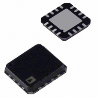
ADA4817-2ACPZ-R2 Analog Devices Inc, ADA4817-2ACPZ-R2 Datasheet - Page 19

ADA4817-2ACPZ-R2
Manufacturer Part Number
ADA4817-2ACPZ-R2
Description
IC, OP-AMP, 1.05GHZ, 870V/µs, LFCSP-16
Manufacturer
Analog Devices Inc
Series
FastFET™r
Specifications of ADA4817-2ACPZ-R2
Op Amp Type
Low Noise
No. Of Amplifiers
2
Bandwidth
1.05GHz
Slew Rate
870V/µs
Supply Voltage Range
5V To 10V
Amplifier Case Style
LFCSP
No. Of Pins
16
Amplifier Type
Voltage Feedback
Number Of Circuits
2
Gain Bandwidth Product
410MHz
-3db Bandwidth
1.05GHz
Current - Input Bias
2pA
Voltage - Input Offset
400µV
Current - Supply
19mA
Current - Output / Channel
40mA
Voltage - Supply, Single/dual (±)
5 V ~ 10 V, ±2.5 V ~ 5 V
Operating Temperature
-40°C ~ 105°C
Mounting Type
Surface Mount
Package / Case
16-LFCSP
Rohs Compliant
Yes
Lead Free Status / RoHS Status
Lead free / RoHS Compliant
Output Type
-
Lead Free Status / RoHS Status
Lead free / RoHS Compliant, Lead free / RoHS Compliant
Available stocks
Company
Part Number
Manufacturer
Quantity
Price
Company:
Part Number:
ADA4817-2ACPZ-R2
Manufacturer:
AD
Quantity:
563
The pole in the loop transmission translates to a zero in the
amplifier’s noise gain, leading to an amplification of the
input voltage noise over frequency. The loop transmission
zero introduced by C
Table 8. RMS Noise Contributions of Photodiode Preamp
Contributor
R
VEN Amp
IEN Amp
F
45
40
35
30
25
20
15
10
–5
5
0
0.1
Figure 46. Photodiode Preamp Frequency Response
G = 63V/V
R
V
V
S
OUT
L
= 100Ω
= 10V
= 6V p-p
Expression
VEN
F
IEN
1
limits the amplification. The noise gain
4
kT
×
×
R
FREQUENCY (MHz)
×
C
F
R
S
×
F
+
×
C
f
10
2
f
M
2
×
C
×
+
. 1
F
. 1
C
57
57
D
+
C
100
F
×
f
3
×
. 1
1000
57
Rev. 0 | Page 19 of 24
bandwidth extends past the preamp signal bandwidth and
is eventually rolled off by the decreasing loop gain of the
amplifier. The current equivalent noise from the inverting
terminal is typically negligible for most applications. The
innovative architecture used in the ADA4817-1/ADA4817-2
makes balancing both inputs unnecessary, as opposed to
traditional FET input amplifiers. Therefore, minimizing the
impedance seen from the noninverting terminal to ground at
all frequencies is critical for optimal noise performance.
Integrating the square of the output voltage noise spectral
density over frequency and then taking the square root allows
users to obtain the total rms output noise of the preamp. Table 8
summarizes approximations for the amplifier and feedback and
source resistances. Noise components for an example preamp
with R
about 6.4 MHz) are also listed.
RMS Noise with R
94 μV
777.5 μV
0.4 μV
783 μV (total)
F
= 50 kΩ, C
S
= 30 pF, and C
F
= 50 kΩ, C
ADA4817-1/ADA4817-2
F
S
= 0.5 pF (bandwidth of
= 30 pF, C
F
= 0.5 pF


