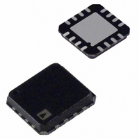
ADA4858-3ACPZ-R2 Analog Devices Inc, ADA4858-3ACPZ-R2 Datasheet - Page 13

ADA4858-3ACPZ-R2
Manufacturer Part Number
ADA4858-3ACPZ-R2
Description
IC, OP-AMP, 600MHZ, 600V/µs, LFCSP-16
Manufacturer
Analog Devices Inc
Datasheet
1.ADA4858-3ACPZ-R7.pdf
(20 pages)
Specifications of ADA4858-3ACPZ-R2
Op Amp Type
High Speed
No. Of Amplifiers
3
Bandwidth
600MHz
Slew Rate
600V/µs
Supply Voltage Range
3V To 5.5V
Amplifier Case Style
LFCSP
No. Of Pins
16
Amplifier Type
Current Feedback
Number Of Circuits
3
-3db Bandwidth
600MHz
Current - Input Bias
8µA
Voltage - Input Offset
500µV
Current - Supply
19mA
Current - Output / Channel
21mA
Voltage - Supply, Single/dual (±)
3 V ~ 5.5 V
Operating Temperature
-40°C ~ 105°C
Mounting Type
Surface Mount
Package / Case
16-LFCSP
Rohs Compliant
Yes
Lead Free Status / RoHS Status
Lead free / RoHS Compliant
Output Type
-
Gain Bandwidth Product
-
Lead Free Status / RoHS Status
Lead free / RoHS Compliant, Lead free / RoHS Compliant
THEORY OF OPERATION
OVERVIEW
The ADA4858-3 is a current feedback amplifier designed for
exceptional performance as a triple amplifier with a variable
gain capability. Its specifications make it especially suitable
for SD and HD video applications. The ADA4858-3 provides
HD video output on a single supply as low as 3.0 V while only
consuming 13 mA per amplifier. It also features a power-down
pin (PD) that reduces the total quiescent current to 2 mA when
activated.
The ADA4858-3 can be used in applications that require both
ac- and dc-coupled inputs and outputs. The output stage on the
ADA4858-3 is capable of driving 2 V p-p video signals into two
doubly terminated video loads (150 Ω each) on a single 5 V supply.
The input range of the ADA4858-3 includes ground, and the
output range is limited by the output headroom set by the voltage
drop across the two diodes from each rail, which occurs 1.2 V
from the positive supply and the charge pump negative supply rails.
CHARGE PUMP OPERATION
The on-board charge pump creates a negative supply for the
amplifier. It provides different negative voltages depending on
the power supply voltage. For a +5 V supply, the negative supply
generated is equal to −3 V with 150 mA of output supply current,
and for a +3.3 V supply, the negative supply is equal to −2 V
with 45 mA of output supply current.
Figure 36 shows the charging cycle when the supply voltage +V
charges C1 through Φ
charges to reach the +V
with switching Φ
When C1 = C2, the charge in C1 is divided between the two
capacitors and slowly increases the voltage in C2 until it reaches
a predetermined voltage (−3 V for +5 V supply and −2 V for
+3.3 V supply). The typical charge pump charging and discharging
frequency is 550 kHz with a 150 Ω load and no input signal;
however, this frequency changes with different loads and supply
conditions.
1
off and switching Φ
CPO
+V
S
Figure 36. C1 Charging Cycle
C2
1
S
to ground. During this cycle, C1 quickly
voltage. The discharge cycle then begins
Φ
1
C1
a
b
2
on, as shown in Figure 37.
Φ
1
Rev. A | Page 13 of 20
S
The ADA4858-3 specifications make it especially suitable for SD
and HD video applications. It also allows dc-coupled video signals
with its black level set to 0 V and its sync tip at −300 mV for
YPbPr video.
The charge pump is always on, even when the power-down pin
(PD) is enabled and the amplifiers are off. However, if a negative
current is not used, the charge pump is in an idle state. Each
amplifier needs −6.3 mA of current, which totals −19 mA for all
three amplifiers. This means additional negative current may be
available by the charge pump for external use. Pin 4 (CPO) is
the charge pump output that provides access to the negative
supply generated by the charge pump.
If the negative supply is used to power another device in the
system, it is only possible for the 5 V supply operation. In the
3.3 V supply operation, the charge pump output current is very
limited. The capacitor C2 placed at the CPO pin, which
regulates the ripple of the negative voltage, can be used as a
coupling capacitor for the external device. However, the charge
pump current should be limited to a maximum of 50 mA for
external use. When powering down the ADA4858-3, the charge
pump is not affected and its output voltage and current are still
available for external use.
It is recommended to use 1 μF low ESR and low ESL capacitors
for C1 and C2. These capactiors should be placed very close to
the part. C1 should be placed between Pin C1_a and Pin C1_b,
and C2 should be placed between Pin CPO and ground. If the
charge pump ripple at the CPO pin is too high, larger capacitors
(that is, 4.7 μF) can replace the 1 μF at C1 and C2.
CPO
+V
Figure 37. C1 Discharging Cycle
S
C2
Φ
2
C1
b
a
Φ
2
ADA4858-3


