LMV934MA National Semiconductor, LMV934MA Datasheet
LMV934MA
Specifications of LMV934MA
Available stocks


Related parts for LMV934MA

LMV934MA Summary of contents
Page 1
... SOIC packages. These small packages are ideal solu- tions for area constrained PC boards and portable electronics such as cellular phones and PDAs. Typical Application © 2010 National Semiconductor Corporation LMV931 Single/LMV932 Dual/ LMV934 Quad Features (Typical 1.8V Supply Values; Unless Otherwise Noted) ■ ...
Page 2
... Absolute Maximum Ratings If Military/Aerospace specified devices are required, please contact the National Semiconductor Sales Office/ Distributors for availability and specifications. ESD Tolerance (Note 2) Machine Model Human Body Model Supply Voltage (V + –V − ) Differential Input Voltage Voltage at Input/Output Pins Storage Temperature Range ...
Page 3
Symbol Parameter V Output Swing O I Output Short Circuit Current O (Note 3) 1.8V AC Electrical Characteristics Unless otherwise specified, all limits guaranteed for T Boldface limits apply at the temperature extremes. See Symbol Parameter SR Slew Rate GBW ...
Page 4
DC Electrical Characteristics Unless otherwise specified, all limits guaranteed for T R > 1 MΩ. Boldface limits apply at the temperature extremes. See L Symbol Parameter V Input Offset Voltage OS TCV Input Offset Voltage Average OS Drift I ...
Page 5
AC Electrical Characteristics Unless otherwise specified, all limits guaranteed for T Boldface limits apply at the temperature extremes. See Symbol Parameter SR Slew Rate GBW Gain-Bandwidth Product Φ Phase Margin m G Gain Margin m e Input-Referred Voltage Noise ...
Page 6
DC Electrical Characteristics Unless otherwise specified, all limits guaranteed for T R > 1 MΩ. Boldface limits apply at the temperature extremes. See L Symbol Parameter V Input Offset Voltage OS TCV Input Offset Voltage Average OS Drift I ...
Page 7
AC Electrical Characteristics Unless otherwise specified, all limits guaranteed for T Boldface limits apply at the temperature extremes. See Symbol Parameter SR Slew Rate GBW Gain-Bandwidth Product Φ Phase Margin m G Gain Margin m e Input-Referred Voltage Noise ...
Page 8
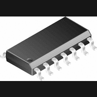
... Units Tape and Reel 1k Units Tape and Reel A86A 3.5k Units Tape and Reel LMV932MA 2.5k Units Tape and Reel LMV934MT 2.5k Units Tape and Reel LMV934MA 2.5k Units Tape and Reel 8 14-Pin TSSOP/SOIC (LMV934) 200326g13 Top View NSC Drawing MAA05A ...
Page 9
Typical Performance Characteristics Supply Current vs. Supply Voltage (LMV931) Sinking Current vs. Output Voltage Output Voltage Swing vs. Supply Voltage Unless otherwise specified, V Sourcing Current vs. Output Voltage 20032622 Output Voltage Swing vs. Supply Voltage 20032628 Gain and Phase ...
Page 10
Gain and Phase vs. Frequency Gain and Phase vs. Frequency PSRR vs. Frequency www.national.com Gain and Phase vs. Frequency 200326g9 CMRR vs. Frequency 200326g11 Input Voltage Noise vs. Frequency 20032656 10 200326g10 20032639 20032658 ...
Page 11
Input Current Noise vs. Frequency 20032666 THD vs. Frequency 20032668 Small Signal Non-Inverting Response 20032670 THD vs. Frequency Slew Rate vs. Supply Voltage Small Signal Non-Inverting Response 11 20032667 20032669 20032671 www.national.com ...
Page 12
Small Signal Non-Inverting Response Large Signal Non-Inverting Response Short Circuit Current vs. Temperature (Sinking) www.national.com Large Signal Non-Inverting Response 20032672 Large Signal Non-Inverting Response 20032674 Short Circuit Current vs. Temperature (Sourcing) 20032676 12 20032673 20032675 20032677 ...
Page 13
Offset Voltage vs. Common Mode Range Offset Voltage vs. Common Mode Range Application Note INPUT AND OUTPUT STAGE The rail-to-rail input stage of this family provides more flexi- bility for the designer. The LMV931/LMV932/LMV934 use a complimentary PNP and NPN ...
Page 14
FIGURE 1. Canceling the Offset Voltage due to Input Bias Current Typical Applications HIGH SIDE CURRENT SENSING The high side current sensing circuit used in a battery charger to monitor charging current to pre- vent over charging. A sense resistor ...
Page 15
... Remember that even with rail-to-rail outputs, the output can not swing past the supplies so the combined common mode voltages plus the signal should not be greater that the sup- plies or limiting will occur. For additional applications, see National Semiconductor application notes AN–29, AN–31, AN–71, and AN–127. -R with R -R ...
Page 16
Simplified Schematic www.national.com 16 200326a9 ...
Page 17
Physical Dimensions inches (millimeters) unless otherwise noted 5-Pin SC70 NS Package Number MAA05A 5-Pin SOT23 NS Package Number MF05A 17 www.national.com ...
Page 18
MSOP NS Package Number MUA08A 8-Pin SOIC NS Package Number M08A 18 ...
Page 19
TSSOP NS Package Number MTC14 14-Pin SOIC NS Package Number M14A 19 www.national.com ...
Page 20
... For more National Semiconductor product information and proven design tools, visit the following Web sites at: www.national.com Products Amplifiers www.national.com/amplifiers Audio www.national.com/audio Clock and Timing www.national.com/timing Data Converters www.national.com/adc Interface www.national.com/interface LVDS www.national.com/lvds Power Management www.national.com/power Switching Regulators www.national.com/switchers LDOs www.national.com/ldo LED Lighting www ...