DS92LV16TVHG National Semiconductor, DS92LV16TVHG Datasheet
DS92LV16TVHG
Specifications of DS92LV16TVHG
Available stocks


Related parts for DS92LV16TVHG

DS92LV16TVHG Summary of contents
Page 1
... The equal and opposite currents through the differential data path control EMI by coupling the resulting fringing fields together. Block Diagram © 2002 National Semiconductor Corporation Features n 25–80 MHz 16:1/1:16 serializer/deserializer (2.56Gbps full duplex throughput) n Independent transmitter and receiver operation with ...
Page 2
... Absolute Maximum Ratings If Military/Aerospace specified devices are required, please contact the National Semiconductor Sales Office/ Distributors for availability and specifications. Supply Voltage ( LVCMOS/LVTTL Input Voltage −0. LVCMOS/LVTTL Output Voltage −0. Bus LVDS Receiver Input Voltage Bus LVDS Driver Output Voltage Bus LVDS Output Short ...
Page 3
Electrical Characteristics Over recommended operating supply and temperature ranges unless otherwise specified. Symbol Parameter Output Differential Voltage V OD (DO+) - (DO-) Output Differential Voltage V OD Unbalance V Offset Voltage OS V Offset Voltage Unbalance OS I Output Short ...
Page 4
Serializer Switching Characteristics Over recommended operating supply and temperature ranges unless otherwise specified. Symbol Parameter ± DO HIGH to t HZD TRI-STATE Delay ± DO LOW to t LZD TRI-STATE Delay ± DO TRI-STATE to t ZHD HIGH Delay ± ...
Page 5
Deserializer Switching Characteristics Over recommended operating supply and temperature ranges unless otherwise specified. Symbol Parameter Conditions Deserializer PLL Lock Time from t DSR1 PWRDWN (with SYNCPAT) (Note 7) Deserializer PLL t Lock time from DSR2 SYNCPAT Ideal Deserializer Figure 16 ...
Page 6
AC Timing Diagrams and Test Circuits FIGURE 1. “Worst Case” Serializer ICC Test Pattern FIGURE 2. “Worst Case” Deserializer ICC Test Pattern FIGURE 3. Serializer Bus LVDS Output Load and Transition Times FIGURE 4. Deserializer CMOS/TTL Output Load and Transition ...
Page 7
AC Timing Diagrams and Test Circuits FIGURE 5. Serializer Input Clock Transition Time FIGURE 7. Serializer TRI-STATE Test Circuit and Timing (Continued) FIGURE 6. Serializer Setup/Hold Times 7 20014307 20014308 20014309 www.national.com ...
Page 8
AC Timing Diagrams and Test Circuits FIGURE 8. Serializer PLL Lock Time, SYNC Timing and PWRDN TRI-STATE Delays www.national.com (Continued) FIGURE 9. Serializer Delay FIGURE 10. Deserializer Delay FIGURE 11. Deserializer Setup and Hold Times 8 20014310 20014311 20014312 20014313 ...
Page 9
AC Timing Diagrams and Test Circuits FIGURE 12. Deserializer TRI-STATE Test Circuit and Timing FIGURE 13. Deserializer PLL Lock Times and PWRDN TRI-STATE Delays (Continued) 9 20014314 20014315 www.national.com ...
Page 10
AC Timing Diagrams and Test Circuits FIGURE 14. Deserializer PLL Lock Time from SyncPAT FIGURE 15. Deterministic Jitter and Ideal Bit Position www.national.com (Continued) 20014329 10 20014322 ...
Page 11
AC Timing Diagrams and Test Circuits t is the noise margin on the left of the above figure negative value to indicate early with respect to ideal. RNMI the noise margin on the right of ...
Page 12
AC Timing Diagrams and Test Circuits www.national.com (Continued) 20014324 FIGURE 19. Icc vs Freq (Rx only) 20014325 FIGURE 20. Icc vs Freq (Tx only) 12 ...
Page 13
Functional Description The DS92LV16 combines a serializer and deserializer onto a single chip. The serializer accepts a 16-bit LVCMOS or LVTTL data bus and transforms it into a BLVDS serial data stream with embedded clock information. The deserializer then recovers ...
Page 14
Resynchronization (Continued) The user can choose to resynchronize to the random data stream or to force fast synchronization by pulsing the Seri- alizer SYNC pin. Since lock time varies due to data stream characteristics, we cannot possibly predict exact lock ...
Page 15
Application Information Lock can be regained at the Deserializer by causing the Serializer to resend SYNC patterns as described above or by random lock which can take more time depending upon the data patterns being received. Input Failsafe In the ...
Page 16
Application Information capacitor is sufficient for these pins. If space is available it 0.01uF may be used in parallel with the 0.1uF capacitor for additional high frequency filtering. GROUNDs The AGND pin should be connected to the signal common in ...
Page 17
... Pin Diagram DS92LV16TVHG Top VIew 17 20014302 www.national.com ...
Page 18
Pin Descriptions Pin # Pin Name 1 RPWDN* 2 REN 3 CONFIG1 4 REFCLK 5, 10, 11, 15 AVDD 6,9,12,16 AGND 7 RIN+ 8 RIN- 13 DO+ 14 DO- 17 TCLK 18 CONFIG2 19 DEN 20 SYNC 21, 22, 23, ...
Page 19
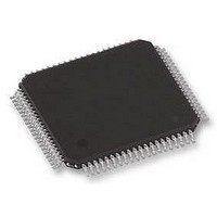
... National does not assume any responsibility for use of any circuitry described, no circuit patent licenses are implied and National reserves the right at any time without notice to change said circuitry and specifications. inches (millimeters) Dimensions shown in millimeters only Order Number DS92LV16TVHG NS Package Number VHG80A 2. A critical component is any component of a life ...