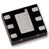
LM3410XSD National Semiconductor, LM3410XSD Datasheet - Page 3

LM3410XSD
Manufacturer Part Number
LM3410XSD
Description
IC, LED DRIVER, POWERWISE 1.6MHZ
Manufacturer
National Semiconductor
Datasheet
1.LM3410XSD.pdf
(32 pages)
Specifications of LM3410XSD
Led Driver Application
Backlighting, LED Flash Driver
No. Of Outputs
1
Output Current
2.8A
Output Voltage
24V
Input Voltage
2.7V To 5.5V
Dimming Control Type
PWM
Topology
Boost, SEPIC
Lead Free Status / RoHS Status
Lead free / RoHS Compliant
Pin Descriptions - 5-Pin SOT23
Pin Descriptions - 6-Pin LLP
Pin Descriptions - 8-Pin eMSOP
DAP
DAP
Pin
Pin
Pin
1
2
3
4
5
1
2
3
4
5
6
1
2
3
4
5
6
7
8
PGND
AGND
PGND
AGND
Name
Name
Name
GND
GND
GND
DIM
DIM
DIM
VIN
SW
VIN
VIN
SW
SW
FB
FB
FB
-
-
Function
No Connect
Power ground pin. Place PGND and output capacitor GND close together.
Supply voltage for power stage, and input supply voltage.
Dimming & shutdown control input. Logic high enables operation. Duty Cycle from 0 to 100%. Do not allow
this pin to float or be greater than VIN + 0.3V.
Feedback pin. Connect FB to external resistor divider to set output voltage.
Signal ground pin. Place the bottom resistor of the feedback network as close as possible to this pin & pin 5
Output switch. Connect to the inductor, output diode.
No Connect
Signal & Power ground. Connect to pin 2 & pin 6 on top layer. Place 4-6 vias from DAP to bottom layer GND
plane.
Function
Output switch. Connect to the inductor, output diode.
Signal and power ground pin. Place the bottom resistor of the feedback network as close as possible to this
pin.
Feedback pin. Connect FB to external resistor divider to set output voltage.
Dimming & shutdown control input. Logic high enables operation. Duty Cycle from 0 to 100%. Do not allow
this pin to float or be greater than VIN + 0.3V.
Supply voltage pin for power stage, and input supply voltage.
Function
Power ground pin. Place PGND and output capacitor GND close together.
Supply voltage for power stage, and input supply voltage.
Dimming & shutdown control input. Logic high enables operation. Duty Cycle from 0 to 100%. Do not allow
this pin to float or be greater than VIN + 0.3V.
Feedback pin. Connect FB to external resistor divider to set output voltage.
Signal ground pin. Place the bottom resistor of the feedback network as close as possible to this pin & pin
4.
Output switch. Connect to the inductor, output diode.
Signal & Power ground. Connect to pin 1 & pin 5 on top layer. Place 4-6 vias from DAP to bottom layer GND
plane.
3
www.national.com


