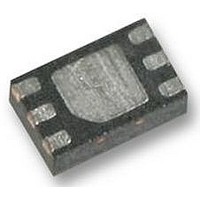
LT3590EDC#PBF Linear Technology, LT3590EDC#PBF Datasheet - Page 11

LT3590EDC#PBF
Manufacturer Part Number
LT3590EDC#PBF
Description
IC, LED DRIVER, BULK MODE, 48V
Manufacturer
Linear Technology
Datasheet
1.LT3590EDCPBF.pdf
(16 pages)
Specifications of LT3590EDC#PBF
Led Driver Application
LED Fixed Signage, Traffic Signs
No. Of Outputs
1
Output Current
50mA
Output Voltage
55V
Input Voltage
4.5V To 55V
Dimming Control Type
PWM / DC
Operating
RoHS Compliant
Topology
Buck
Available stocks
Company
Part Number
Manufacturer
Quantity
Price
The dimming range can be further extended by changing
the amplitude of the PWM signal. The height of the PWM
signal sets the commanded sense voltage across the sense
resistor through the CTRL pin. In this manner both analog
dimming and direct PWM dimming extend the dimming
range for a given application. The color of the LEDs no
longer remains constant because the forward current of
the LED changes with the height of the CTRL signal. For
the ten LED application described above, the LEDs can be
dimmed fi rst, modulating the duty cycle of the PWM signal.
Once the minimum duty cycle is reached, the height of the
PWM signal can be decreased below 1.5V down to 150mV.
The use of both techniques together allows the average
LED current for the ten LED application to be varied from
50mA down to less than 50μA.
APPLICATIONS INFORMATION
CTRL
V
REG
V
IN
LED
V
REG
V
IN
R1
(a) SC70 Package
5
6
7
8
OUT
C3
CTRL
C1
C2
L1
SW
4
3
2
1
Figure 8. Recommended Component Placement
GND
GND
CTRL
Internal Voltage Regulator
The LT3590 has a 3.3V onboard voltage regulator capable
of sourcing up to 1mA of current for use by an external
device. This feature may be used to power-up a controller
from the LT3590. The 3.3V is available even during shut-
down. It is required to place a 0.1μF capacitor from V
to ground. The regulator current is limited to 1.5mA.
Board Layout Considerations
As with all switching regulators, careful attention must be
paid to the PCB board layout and component placement.
To prevent electromagnetic interference (EMI) problems,
proper layout of high frequency switching paths is essen-
tial. Minimize the length and area of all traces connected
to the switching node pin (SW). Keep the sense voltage
pins (V
the output capacitor, C2, next to the V
a ground plane under the switching regulator to minimize
interplane coupling. Recommended component placement
is shown in Figure 8.
IN
GND
and LED) away from the switching node. Place
CTRL
GND
(b) 2mm × 2mm DFN Package
SW
1
2
3
L1
C1
7
C3
OUT
6
5
4
C2
V
IN
V
R1
REG
IN
pin. Always use
LED
LT3590
3590 F08
11
GND
V
V
REG
IN
REG
3590f


