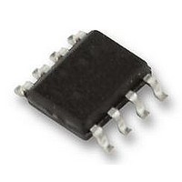
LM27222M National Semiconductor, LM27222M Datasheet

LM27222M
Specifications of LM27222M
Available stocks
Related parts for LM27222M
LM27222M Summary of contents
Page 1
... Vin and Vcc are stable and the switching controller starts operating. To support low power states in notebook Typical Application © 2004 National Semiconductor Corporation systems, LM27222 draws only 5µA from the 5V rail when the IN and LEN inputs are low or floating. ...
Page 2
... Connection Diagram Ordering Information Order Number Size NSC Drawing # LM27222M SO-8 LM27222MX LM27222SD LLP-8 LM27222SDX Pin Description Pin # Pin Name 1 SW High-side driver return. Should be connected to the common node of high and low-side MOSFETs High-side gate drive output. Should be connected to the high-side MOSFET gate. Pulled down internally to SW with a 10K resistor to prevent spurious turn on of the high-side MOSFET when the driver is off ...
Page 3
Block Diagram 20117903 3 www.national.com ...
Page 4
... Absolute Maximum Ratings If Military/Aerospace specified devices are required, please contact the National Semiconductor Sales Office/ Distributors for availability and specifications GND GND GND (Note 2) LEN to GND IN to GND LG to GND HG to GND Electrical Characteristics VCC = GND = 0V, unless otherwise specified. Typicals and limits appearing in plain type apply for T +25˚ ...
Page 5
Electrical Characteristics VCC = GND = 0V, unless otherwise specified. Typicals and limits appearing in plain type apply for T +25˚C. Limits appearing in boldface type apply over the entire operating temperature range (-40˚C ≤ ...
Page 6
Typical Waveforms FIGURE 2. IN Rising The typical waveforms are from a circuit similar to Figure 1 with: Q1 Si7390DP Q2 Si7356DP L1: 0.4 µ 12V IN www.national.com 20117907 FIGURE 3. IN Falling 20117909 ...
Page 7
Application Information MINIMUM PULSE WIDTH As the input pulse width to the IN pin is decreased, the pulse width of the high-side gate drive (HG-SW) also decreases. However, for input pulse widths 60ns and smaller, the HG-SW remains constant at ...
Page 8
Application Information used, and secondly, high-side switch resistance becomes a larger loss factor than the switching losses. Of course with a lower input voltage, the input capacitor voltage rating can be reduced and the inductor value can be reduced as ...
Page 9
9 www.national.com ...
Page 10
... Physical Dimensions unless otherwise noted www.national.com inches (millimeters) 8-Lead Small Outline Package Order Number: LM27222M, LM27222MX NS Package Number M08A 8-Lead LLP Package Order Number: LM27222SD, LM27222SDX NS Package Number SDC08A 10 ...
Page 11
... BANNED SUBSTANCE COMPLIANCE National Semiconductor certifies that the products and packing materials meet the provisions of the Customer Products Stewardship Specification (CSP-9-111C2) and the Banned Substances and Materials of Interest Specification (CSP-9-111S2) and contain no ‘‘Banned Substances’’ as defined in CSP-9-111S2. ...


