ADM3101EACPZ-250R7 Analog Devices Inc, ADM3101EACPZ-250R7 Datasheet - Page 8
ADM3101EACPZ-250R7
Manufacturer Part Number
ADM3101EACPZ-250R7
Description
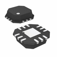
IC, RS-232 TXRX, 460KBPS, 5.5V, LFCSP-12
Manufacturer
Analog Devices Inc
Type
Transceiverr
Datasheet
1.ADM3101EACPZ-REEL.pdf
(12 pages)
Specifications of ADM3101EACPZ-250R7
Device Type
Transceiver
Ic Interface Type
RS232
No. Of Drivers
1
Supply Voltage Range
3V To 5.5V
Driver Case Style
LFCSP
No. Of Pins
12
Operating Temperature Range
-40°C To +85°C
Number Of Drivers/receivers
1/1
Protocol
RS232
Voltage - Supply
3 V ~ 3.6 V
Mounting Type
Surface Mount
Package / Case
12-LFCSP
Data Rate
460Kbps
Number Of Receivers
1
Number Of Transmitters
1
Number Of Transceivers
1
Receiver Signal Type
Single-Ended
Transmitter Signal Type
Single-Ended
Single Supply Voltage (typ)
3.3V
Single Supply Voltage (min)
3V
Single Supply Voltage (max)
5.5V
Dual Supply Voltage (typ)
Not RequiredV
Dual Supply Voltage (min)
Not RequiredV
Dual Supply Voltage (max)
Not RequiredV
Supply Current
5mA
Power Supply Requirement
Single
Operating Temp Range
-40C to 85C
Operating Temperature Classification
Industrial
Mounting
Surface Mount
Pin Count
12
Package Type
LFCSP EP
Lead Free Status / RoHS Status
Lead free / RoHS Compliant
Lead Free Status / RoHS Status
Lead free / RoHS Compliant, Lead free / RoHS Compliant
Other names
ADM3101EACPZ-250R7TR
Available stocks
Company
Part Number
Manufacturer
Quantity
Price
Company:

Part Number:
ADM3101EACPZ-250R7
Manufacturer:
INFINEON
Quantity:
101
Part Number:
ADM3101EACPZ-250R7
Manufacturer:
ADI/亚德诺
Quantity:
20 000


ADM3101E
THEORY OF OPERATION
The ADM3101E is a single-channel RS-232 line driver/receiver.
Step-up voltage converters, coupled with level shifting trans-
mitters and receivers, allow RS-232 levels to be developed while
operating from a single 3.3 V supply.
CMOS technology is used to keep the power dissipation to
an absolute minimum, allowing maximum battery life in
portable applications.
CIRCUIT DESCRIPTION
The internal circuitry consists of the following main sections:
•
•
•
Charge Pump Voltage Converter
The charge pump voltage converter consists of a 200 kHz oscil-
lator and a switching matrix. The converter generates a ±6.6 V
supply (when unloaded) from the 3.3 V input level. This is achieved
in two stages by using a switched capacitor technique, as illustrated
in Figure 13 and Figure 14. First, the 3.3 V input supply is doubled
to +6.6 V by using C1 as the charge storage element. The +6.6 V
level is then inverted to generate −6.6 V using C2 as the storage
element. C3 is shown connected between V+ and V
equally effective if connected between V+ and GND.
The C3 and C4 capacitors are used to reduce the output ripple.
The values are not critical and can be increased, if desired. Larger
capacitors (up to 10 μF) can also be used in place of the C1, C2,
C3, and C4 capacitors.
0.1µF
0.1µF
*INTERNAL 5kΩ PULL-DOWN
RESISTOR ON THE RS-232 INPUT.
16V
16V
C1
C2
A charge pump voltage converter
A 3.3 V logic to an EIA/TIA-232E transmitter
An EIA/TIA-232E to a 3.3 V logic receiver
OUTPUT
+
+
CMOS
INPUT
CMOS
OSCILLATOR
GND
INTERNAL
V
CC
C1+
C1–
C2+
C2–
T
R
Figure 13. Charge Pump Voltage Doubler
IN
OUT
Figure 12. Typical Operating Circuit
VOLTAGE DOUBLER
VOLTAGE INVERTER
S1
S2
+3.3V TO +6.6V
+6.6V TO –6.6V
ADM3101E
GND
T
R
+
C1
S3
S4
T
V
OUT
R
V+
CC
V–
IN
+3.3V INPUT
+
EIA/TIA-232E
OUTPUT
EIA/TIA-232E
INPUT*
C3
+
+
C3
0.1µF
6.3V
C4
0.1µF
16V
V+ = 2V
V
CC
CC
but is
+
CC
C5
0.1µF
Rev. C | Page 8 of 12
3.3 V Logic to EIA/TIA-232E Transmitter
The transmitter driver converts the 3.3 V logic input levels
into RS-232 output levels. When driving an RS-232 load with
V
the T
open-drain output, but the maximum operating data rate is
reduced when the T
EIA/TIA-232E to 3.3 V Logic Receiver
The receiver is an inverting level shifter that accepts the RS-232
input level and translates it into a 3.3 V logic output level. The
input has an internal 5 kΩ pull-down resistor to ground and is
protected against overvoltages of up to ±30 V. An unconnected
input is pulled to 0 V by the internal 5 kΩ pull-down resistor,
which, therefore, results in a Logic 1 output level for an uncon-
nected input or for an input connected to GND.
The receiver has a Schmitt trigger input with a hysteresis level
of 0.4 V, which ensures error-free reception for both a noisy
input and for an input with slow transition times.
CMOS Input Voltage Thresholds
The CMOS input and output pins (T
ADM3101E are designed to interface with 1.8 V logic
thresholds when V
The CMOS input and output pins (T
ADM3101E are also designed to interface with TTL/CMOS
logic thresholds when V
ESD Protection on RS-232 and CMOS I/O Pins
All RS-232 (T
and outputs are protected against electrostatic discharges (up
to ±15 kV).
HIGH BAUD RATE
The ADM3101E features high slew rates, permitting data trans-
mission at rates well in excess of the EIA/RS-232 specifications.
The RS-232 voltage levels are maintained at data rates of up to
460 kbps, even under worst-case loading conditions, when T
driven by a push-pull output. The slew rate is internally controlled
to less than 30 V/μs to minimize EMI interference.
CC
DOUBLER
VOLTAGE
= 3.3 V, the output voltage swing is typically ±6 V. Internally,
IN
FROM
pin has a weak pull-up that allows it to be driven by an
OSCILLATOR
GND
INTERNAL
V+
OUT
Figure 14. Charge Pump Voltage Inverter
and R
CC
IN
= 3.3 V.
pin is driven by an open-drain pin.
S1
S2
IN
CC
) and CMOS (T
= 5 V.
+
C2
IN
IN
S3
S4
and R
and R
IN
and R
OUT
OUT
+
C4
) of the
) of the
OUT
) inputs
GND
V– = –(V+)
IN
is
Related parts for ADM3101EACPZ-250R7
Image
Part Number
Description
Manufacturer
Datasheet
Request
R

Part Number:
Description:
?15 Kv Esd Protected, 3.3 V Single-channel Rs-232 Line Driver/receiver
Manufacturer:
Analog Devices, Inc.
Datasheet:

Part Number:
Description:
±1.7g Dual-Axis IMEMS Accelerometer Evaluation Board
Manufacturer:
Analog Devices Inc
Datasheet:

Part Number:
Description:
Inertial Sensor Evaluation System
Manufacturer:
Analog Devices Inc
Datasheet:
Part Number:
Description:
Manufacturer:
Analog Devices Inc
Datasheet:
Part Number:
Description:
Manufacturer:
Analog Devices Inc
Datasheet:
Part Number:
Description:
Manufacturer:
Analog Devices Inc
Datasheet:
Part Number:
Description:
Manufacturer:
Analog Devices Inc
Datasheet:
Part Number:
Description:
Manufacturer:
Analog Devices Inc
Datasheet:
Part Number:
Description:
Manufacturer:
Analog Devices Inc
Datasheet:
Part Number:
Description:
Manufacturer:
Analog Devices Inc
Datasheet:
Part Number:
Description:
Manufacturer:
Analog Devices Inc
Datasheet:
Part Number:
Description:
Manufacturer:
Analog Devices Inc
Datasheet:
Part Number:
Description:
Manufacturer:
Analog Devices Inc
Datasheet: