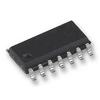
DS14C88M National Semiconductor, DS14C88M Datasheet - Page 3

DS14C88M
Manufacturer Part Number
DS14C88M
Description
LINE DRIVER QUAD RS232, SMD, 14C88
Manufacturer
National Semiconductor
Datasheet
1.DS14C88M.pdf
(6 pages)
Specifications of DS14C88M
Device Type
Line
No. Of Drivers
4
Supply Voltage Range
± 4.5V To ± 12.6V
Driver Case Style
SOIC
No. Of Pins
14
Operating Temperature Range
0°C To +75°C
Svhc
No SVHC (15-Dec-2010)
Operating
RoHS Compliant
Interface Type
RS232
Rohs Compliant
Yes
Available stocks
Company
Part Number
Manufacturer
Quantity
Price
Part Number:
DS14C88M
Manufacturer:
NS/国半
Quantity:
20 000
Company:
Part Number:
DS14C88M/NOPB
Manufacturer:
NSC
Quantity:
1 776
Company:
Part Number:
DS14C88MX
Manufacturer:
MOLEX
Quantity:
1 000
Part Number:
DS14C88MX
Manufacturer:
NS/国半
Quantity:
20 000
Company:
Part Number:
DS14C88MX/NOPB
Manufacturer:
TI
Quantity:
16 700
Company:
Part Number:
DS14C88MX/NOPB
Manufacturer:
NS
Quantity:
75
Part Number:
DS14C88MX/NOPB
Manufacturer:
TI/德州仪器
Quantity:
20 000
Company:
Part Number:
DS14C88MX/NOPB
Manufacturer:
NSC
Quantity:
14 519
t
t
t
t
tsk
S
PLH
PHL
r
f
R
Switching Characteristics
Over Recommended Operating Conditions, unless otheriwse specified (Figures 2, 3)
Note 1: “Absolute Maximum Ratings” are those values beyond which the safety of the device cannot be guaranteed. They are not meant to imply that the devices
should be operated at these limits. The tables of “Electrical Characteristics” specify conditions for device operation.
Note 2: Derate N Package 12.1 mW/˚C, and M Package 8.5 mW/˚C above +25˚C.
Note 3: I
Note 4: Power supply (V
Note 5: AC input test waveforms for test purposes: t
Note 6: Input rise and rall times must not exceed 5 µs.
Note 7: The output slew rate, rise time, and fall time are measured from the +3.0V to the −3.0V level on the output waveform.
Note 8: C
Note 9: ESD Rating (HBM, 1.5 kΩ, 100 pF) ≥ 1.0 kV.
Parameter Measure Information
Symbol
OS+
L
include jig and probe capacitances.
and I
Propagation Delay
Low to High
Propagation Delay
High to Low
Rise Time (Note 7)
Fall Time (Note 7)
Typical Propagation
Delay Skew
Output Slew Rate
(Note 7)
OS−
values are for one output at a time. If more than one output is shorted simultaneously, the device dissipation may be exceeded.
+
, V
Parameter
−
) and GND pins are connected to ground for the Output Resistance Test (R
FIGURE 1. Output Resistance Test Circuit (Power-Off)
r
FIGURE 2. Driver Load Circuit (Note 8)
= t
(Notes 5, 6)
V
V
V
V
V
V
V
V
V
R
C
f
+
+
+
+
+
+
+
+
+
≤ 20 ns, V
L
L
= +4.5V, V
= +9.0V, V
= +12V, V
= +4.5V, V
= +9.0V, V
= +12V, V
= +4.5V, V
= +9.0V, V
= +12V, V
= 3 kΩ to 7 kΩ
= 15 pF to 2500 pF
Conditions
IH
= 2V, V
−
−
−
−
−
−
−
−
−
= −12V
= −12V
= −12V
= −4.5V
= −9.0V
= −4.5V
= −9.0V
= −4.5V
= −9.0V
IL
3
= 0.8V (0.6V at V
+
01110503
= 4.5V, V
Min
0.2
0.2
O
).
−
= −4.5V)
1.35
Typ
250
200
150
1.5
1.2
1.2
1.5
1.3
1.0
1.0
01110502
Max
6.0
5.0
4.0
6.0
5.0
4.0
30
www.national.com
Units
V/µs
µs
µs
µs
µs
µs
µs
µs
µs
ns
ns
ns


