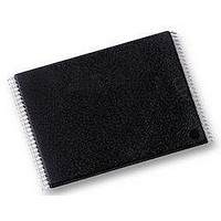
S29GL064A10TFIR20 Spansion Inc., S29GL064A10TFIR20 Datasheet - Page 47

S29GL064A10TFIR20
Manufacturer Part Number
S29GL064A10TFIR20
Description
Flash - NOR IC
Manufacturer
Spansion Inc.
Datasheet
1.S29GL064M90TFIR00.pdf
(79 pages)
Specifications of S29GL064A10TFIR20
Memory Size
64Mbit
Memory Configuration
64K X 16
Ic Interface Type
Parallel
Access Time
100ns
Memory Case Style
TSOP
No. Of Pins
48
Page/burst Read Access
25ns
Supply Voltage Max
3.6V
Sector Type
Uniform
Lead Free Status / RoHS Status
Lead free / RoHS Compliant
10.6
November 16, 2007 S29GL-N_01_09
Chip Erase Command Sequence
Chip erase is a six bus cycle operation. The chip erase command sequence is initiated by writing two unlock
cycles, followed by a set-up command. Two additional unlock write cycles are then followed by the chip erase
command, which in turn invokes the Embedded Erase algorithm. The device does not require the system to
preprogram prior to erase. The Embedded Erase algorithm automatically preprograms and verifies the entire
memory for an all zero data pattern prior to electrical erase. The system is not required to provide any
controls or timings during these operations.
address and data requirements for the chip erase command sequence.
When the Embedded Erase algorithm is complete, the device returns to the read mode and addresses are no
longer latched. The system can determine the status of the erase operation by using DQ7, DQ6, or DQ2.
Refer to
Any commands written during the chip erase operation are ignored. However, note that a hardware reset
immediately terminates the erase operation. If this occurs, the chip erase command sequence should be
reinitiated once the device returns to reading array data, to ensure data integrity.
Figure 10.4 on page 49
parameters, and
Write Operation Status on page 55
Figure 15.7 on page 69
No
illustrates the algorithm for the erase operation. Refer to
D a t a
Sequence in Progress
Program Operation
Write address/data
Write address/data
Program Suspend
or Write-to-Buffer
operation prior to
Device reverts to
S29GL-N MirrorBit
Figure 10.3 Program Suspend/Program Resume
Read data as
XXXh/B0h
Wait 20 μs
XXXh/30h
reading?
required
Done
S h e e t
Yes
for timing diagrams.
Table 10.1 on page 51
for information on these status bits.
®
Flash Family
Write Program Suspend
Command Sequence
Command is also valid for
Erase-suspended-program
operations
Autoselect and SecSi Sector
read operations are also allowed
Data cannot be read from erase- or
program-suspended sectors
Write Program Resume
Command Sequence
and
Table 10.3 on page 53
Table 15.3 on page 67
show the
for
47


