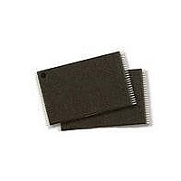
S29JL032H90TFI320 Spansion Inc., S29JL032H90TFI320 Datasheet - Page 57

S29JL032H90TFI320
Manufacturer Part Number
S29JL032H90TFI320
Description
IC, FLASH, 32MBIT, 90NS, TSOP-48
Manufacturer
Spansion Inc.
Datasheet
1.S29JL032H90TFI320.pdf
(61 pages)
Specifications of S29JL032H90TFI320
Memory Type
Flash
Memory Size
32Mbit
Memory Configuration
4M X 8 / 2M X 16
Ic Interface Type
CFI, Parallel
Access Time
90ns
Supply Voltage Range
2.7 To 3.6 V
Memory Case Style
TSOP
Data Bus Width
8 bit, 16 bit
Architecture
Boot Sector
Interface Type
Conventional
Supply Voltage (max)
3.6 V
Supply Voltage (min)
2.7 V
Maximum Operating Current
2 mA
Mounting Style
SMD/SMT
Operating Temperature
+ 85 C
Package / Case
TSOP-48
Rohs Compliant
YES
No. Of Pins
48
Lead Free Status / RoHS Status
Lead free / RoHS Compliant
Lead Free Status / RoHS Status
Lead free / RoHS Compliant, Lead free / RoHS Compliant
Available stocks
Company
Part Number
Manufacturer
Quantity
Price
Company:
Part Number:
S29JL032H90TFI320
Manufacturer:
Spansion
Quantity:
135
Company:
Part Number:
S29JL032H90TFI320
Manufacturer:
PANASONIC
Quantity:
4 314
Part Number:
S29JL032H90TFI320
Manufacturer:
SPANSION
Quantity:
20 000
18. Erase and Programming Performance
19. TSOP Pin Capacitance
August 31, 2009 S29JL032H_00_B8
Notes
1. Typical program and erase times assume the following conditions: 25°C, V
2. Under worst case conditions of 90°C, V
3. The typical chip programming time is considerably less than the maximum chip programming time listed, since most bytes program faster
4. In the pre-programming step of the Embedded Erase algorithm, all bytes are programmed to 00h before erasure.
5. System-level overhead is the time required to execute the two- or four-bus-cycle sequence for the program command. See
6. The device has a minimum cycling endurance of 100,000 cycles per sector.
Notes
1. Sampled, not 100% tested.
2. Test conditions T
Sector Erase Time
Chip Erase Time
Byte Program Time
Word Program Time
Accelerated Byte/Word Program Time
Chip Program Time
(Note 3)
than the maximum program times listed.
on page 37
Parameter Symbol
C
C
C
OUT
IN2
IN
for further information on command definitions.
A
= 25°C, f = 1.0 MHz.
Parameter
Byte Mode
Word Mode
Accelerated Mode
D a t a
Control Pin Capacitance
Parameter Description
Output Capacitance
Input Capacitance
CC
S h e e t
= 2.7 V, 1,000,000 cycles.
S29JL032H
Typ
12.6
12.0
(Note 1)
0.4
28
10
4
6
4
V
V
V
OUT
IN
IN
Max
CC
= 0
= 0
= 0
= 3.0 V, 100,000 cycles; checkerboard data pattern.
100
(Note 2)
Test Setup
80
70
50
35
30
5
TSOP
TSOP
TSOP
Unit
sec
sec
sec
µs
µs
µs
Excludes 00h programming
Typ
8.5
7.5
prior to erasure
6
Excludes system level
overhead
Comments
Max
7.5
12
9
(Note 5)
Table 10.1
(Note 4)
Unit
pF
pF
pF
57


