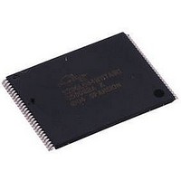
S29GL128P11TFI010 Spansion Inc., S29GL128P11TFI010 Datasheet - Page 28

S29GL128P11TFI010
Manufacturer Part Number
S29GL128P11TFI010
Description
IC, FLASH, 128MBIT, 110NS, TSOP-56
Manufacturer
Spansion Inc.
Datasheet
1.S29GL128P11TFI010.pdf
(79 pages)
Specifications of S29GL128P11TFI010
Memory Type
Flash
Memory Size
128Mbit
Ic Interface Type
Parallel
Access Time
110ns
Supply Voltage Range
2.7V To 3.6V
Memory Case Style
TSOP
No. Of Pins
56
Data Bus Width
8 bit, 16 bit
Architecture
Sectored
Interface Type
Serial
Supply Voltage (max)
3.6 V
Supply Voltage (min)
2.7 V
Maximum Operating Current
50 mA
Mounting Style
SMD/SMT
Operating Temperature
+ 85 C
Package / Case
TSOP-56
Lead Free Status / RoHS Status
Lead free / RoHS Compliant
Lead Free Status / RoHS Status
Lead free / RoHS Compliant, Lead free / RoHS Compliant
Available stocks
Company
Part Number
Manufacturer
Quantity
Price
Company:
Part Number:
S29GL128P11TFI010
Manufacturer:
Spansion
Quantity:
135
Company:
Part Number:
S29GL128P11TFI010
Manufacturer:
SPANSION
Quantity:
709
Part Number:
S29GL128P11TFI010
Manufacturer:
SPANSION
Quantity:
20 000
28
Software Functions and Sample Code
Notes
1. Base = Base Address.
2. Last = Last cycle of write buffer program operation; depending on number of words written, the total number of cycles may be from 6 to
3. For maximum efficiency, it is recommended that the write buffer be loaded with the highest number of words (N words) possible.
The following is a C source code example of using the write buffer program function. Refer to the Spansion
Low Level Driver User’s Guide (available on www.spansion.com) for general information on Spansion Flash
memory software development guidelines.
Cycle
5 to 36
Last
37.
/* Example: Write Buffer Programming Command
/* NOTES: Write buffer programming limited to 16 words. */
/*
/*
/*
/*
for (i=0;i<=wc;i++)
{
*dst++ = *src++; /* ALL dst MUST BE in same Write Buffer */
}
*( (UINT16 *)sector_address )
/* Example: Write Buffer Abort Reset */
1
2
3
4
UINT16 *src = source_of_data;
UINT16 *dst = destination_of_data;
UINT16 wc
*( (UINT16 *)base_addr + 0x555 ) = 0x00AA;
*( (UINT16 *)base_addr + 0x2AA ) = 0x0055;
*( (UINT16 *)sector_address )
*( (UINT16 *)sector_address )
/* poll for completion */
*( (UINT16 *)addr + 0x555 ) = 0x00AA;
*( (UINT16 *)addr + 0x2AA ) = 0x0055;
*( (UINT16 *)addr + 0x555 ) = 0x00F0;
Description
Write Buffer Load Command
Number of words (N) loaded into the write buffer can be from 1 to 32 words (1 to 64 bytes).
All addresses to be written to the flash in
one operation must be within the same flash
page. A flash page begins at addresses
evenly divisible by 0x20.
Write Buffer to Flash
Load Buffer Word N
Write Word Count
= words_to_program -1;
(LLD Functions Used = lld_WriteToBufferCmd, lld_ProgramBufferToFlashCmd)
Unlock
Unlock
S29GL-P MirrorBit
= 0x0029;
Table 7.7 Write Buffer Program
Operation
= 0x0025;
= wc;
Write
Write
Write
Write
Write
Write
D a t a
®
/* write unlock cycle 1
/* write unlock cycle 2
/* write buffer abort reset
Flash Family
/* write confirm command
/* flash destination address
/* address of source data
/* word count (minus 1)
/* write unlock cycle 1
/* write unlock cycle 2
/* write write buffer load command */
/* write word count (minus 1)
Byte Address
Base + AAAh
S h e e t
Base + 555h
Program Address, Word N
*/
*/
*/
*/
*/
Sector Address
Sector Address
Sector Address
Word Address
Base + 2AAh
Base + 555h
S29GL-P_00_A11 June 11, 2008
*/
*/
*/
*/
*/
Data
*/
*/
*/
*/
*/
Word Count (N–1)h
Word N
00AAh
0055h
0025h
0029h


