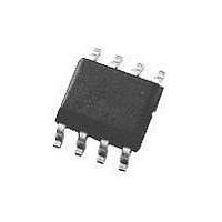
LM2594M-5.0 National Semiconductor, LM2594M-5.0 Datasheet - Page 8

LM2594M-5.0
Manufacturer Part Number
LM2594M-5.0
Description
IC, STEP-DOWN REGULATOR, 8-SOIC
Manufacturer
National Semiconductor
Datasheet
1.LM2594MX-5.0NOPB.pdf
(28 pages)
Specifications of LM2594M-5.0
Primary Input Voltage
12V
No. Of Outputs
1
Output Voltage
5V
Output Current
500mA
No. Of Pins
8
Operating Temperature Range
-40°C To +125°C
Supply Voltage Range
4.5V To 40V
Termination Type
SMD
Dc To Dc Converter Type
Inverting/Step Down
Number Of Outputs
1
Pin Count
8
Input Voltage
40V
Switching Freq
173kHz
Efficiency
82%
Package Type
SOIC N
Output Type
Fixed
Switching Regulator
Yes
Mounting
Surface Mount
Input Voltage (min)
4.5V
Operating Temp Range
-40C to 125C
Operating Temperature Classification
Automotive
Filter Terminals
SMD
Rohs Compliant
No
Input Voltage Primary Max
40V
Lead Free Status / RoHS Status
Contains lead / RoHS non-compliant
Lead Free Status / RoHS Status
Contains lead / RoHS non-compliant
Available stocks
Company
Part Number
Manufacturer
Quantity
Price
Company:
Part Number:
LM2594M-5.0
Manufacturer:
NS
Quantity:
5 000
Company:
Part Number:
LM2594M-5.0
Manufacturer:
NS
Quantity:
10
Part Number:
LM2594M-5.0
Manufacturer:
NS/国半
Quantity:
20 000
Company:
Part Number:
LM2594M-5.0/NOPB
Manufacturer:
TI
Quantity:
4 540
Company:
Part Number:
LM2594M-5.0/NOPB
Manufacturer:
NS
Quantity:
480
Part Number:
LM2594M-5.0/NOPB
Manufacturer:
NS/国半
Quantity:
20 000
www.national.com
Typical Circuit and Layout Guidelines
C
C
D1 — 1A, 40V Schottky Rectifier, 1N5819
L1 — 100 µH, L20
Select components with higher voltage ratings for designs using the LM2594HV with an input voltage between 40V and 60V.
C
C
D1 — 1A, 40V Schottky Rectifier, 1N5819
L1 — 100 µH, L20
R
C
As in any switching regulator, layout is very important. Rap-
idly switching currents associated with wiring inductance can
generate voltage transients which can cause problems. For
minimal inductance and ground loops, the wires indicated by
heavy lines should be wide printed circuit traces and
should be kept as short as possible. For best results, ex-
ternal components should be located as close to the
switcher lC as possible using ground plane construction or
single point grounding.
IN
OUT
IN
OUT
1
FF
— 1 k , 1%
— 68 µF, 35V, Aluminum Electrolytic Nichicon “PL Series”
— 68 µF, 35V, Aluminum Electrolytic Nichicon “PL Series”
— See Application Information Section
— 120 µF, 25V Aluminum Electrolytic, Nichicon “PL Series”
— 120 µF, 25V Aluminum Electrolytic, Nichicon “PL Series”
FIGURE 1. Typical Circuits and Layout Guides
Adjustable Output Voltage Versions
Fixed Output Voltage Versions
8
If open core inductors are used, special care must be
taken as to the location and positioning of this type of induc-
tor. Allowing the inductor flux to intersect sensitive feedback,
lC groundpath and C
When using the adjustable version, special care must be
taken as to the location of the feedback resistors and the as-
sociated wiring. Physically locate both resistors near the IC,
and route the wiring away from the inductor, especially an
open core type of inductor. (See application section for more
information.)
OUT
wiring can cause problems.
DS012439-23
DS012439-22


