LM2587S-5.0 National Semiconductor, LM2587S-5.0 Datasheet
LM2587S-5.0
Specifications of LM2587S-5.0


Related parts for LM2587S-5.0


LM2587S-5.0 Summary of contents
Page 1
... Flyback regulator n Multiple-output regulator n Simple boost regulator ± 4%, within specified n Forward converter NSC Package Drawing T05D LM2587T-3.3, LM2587T-5.0, LM2587T-12, LM2587T-ADJ TS5B LM2587S-3.3, LM2587S-5.0, LM2587S-12, LM2587S-ADJ TS5B LM2587SX-3.3, LM2587SX-5.0, LM2587SX-12, LM2587SX-ADJ DS012316 February 2004 ± 4% max over line 01231601 Order Number www.national.com ...
Page 2
... Absolute Maximum Ratings If Military/Aerospace specified devices are required, please contact the National Semiconductor Sales Office/ Distributors for availability and specifications. Input Voltage Switch Voltage Switch Current (Note 2) Compensation Pin Voltage Feedback Pin Voltage Storage Temperature Range Lead Temperature (Soldering, 10 sec.) LM2587-3.3 ...
Page 3
LM2587-5.0 Electrical Characteristics Symbol Parameters Voltage V ∆V Reference Voltage V REF Line Regulation G Error Amp I M COMP Transconductance V A Error Amp V VOL Voltage Gain R LM2587-12 Electrical Characteristics Specifications with standard type face are for ...
Page 4
LM2587-ADJ Electrical Characteristics Symbol Parameters ∆V Reference Voltage V REF Line Regulation G Error Amp I M Transconductance V A Error Amp V VOL Voltage Gain R I Error Amp V B Input Bias Current All Output Voltage Versions Electrical ...
Page 5
All Output Voltage Versions Electrical Characteristics Symbol Parameters θ S Package, Junction to Ambient (Note 12) JA θ S Package, Junction to Ambient (Note 13) JA θ S Package, Junction to Ambient (Note 14) JA θ S Package, Junction to ...
Page 6
Typical Performance Characteristics ∆Reference Voltage vs Supply Voltage Current Limit vs Temperature Switch Saturation Voltage vs Temperature www.national.com (Continued) 01231650 01231652 Switch Transconductance 01231654 6 Supply Current vs Switch Current 01231651 Feedback Pin Bias Current vs Temperature 01231653 vs Temperature ...
Page 7
... TO-263 (S) Top View 01231605 (Continued) 01231656 01231658 01231603 Order Number LM2587T-3.3, LM2587T-5.0, LM2587T-12 or LM2587T-ADJ See NS Package Number T05D Order Number LM2587S-3.3, LM2587S-5.0, LM2587S-12 or LM2587S-ADJ See NS Package Number TS5B 7 Error Amp Transconductance vs Temperature 01231657 Short Circuit Frequency vs Temperature 01231659 Bent, Staggered Leads ...
Page 8
Block Diagram For Fixed Versions3.3V 3.4k 2k5V 6.15k 2k12V 8.73k 1kFor Adj. VersionR1 = Short (0Ω), R2 = Open Test Circuits C — 100 µF, 25V Aluminum ElectrolyticC ...
Page 9
Test Circuits (Continued) C — 100 µF, 25V Aluminum ElectrolyticC — 0.1 µF CeramicL — 15 µH, Renco #RL-5472-5D — 1N5820C IN1 IN2 ElectrolyticC — 0.47 µF CeramicR — 2kFor 12V Devices Short (0Ω) and R ...
Page 10
Flyback Regulator Operation The LM2587 is ideally suited for use in the flyback regulator topology. The flyback regulator can produce a single output voltage, such as the one shown in Figure 4, or multiple output voltages. In Figure 4, the ...
Page 11
Typical Performance Characteristics A: Switch Voltage, 10 V/divB: Switch Current, 5 A/divC: Output Rectifier Current, 5 A/divD: Output Ripple Voltage, 100 mV/div AC-Coupled Horizontal: 2 µs/div Typical Flyback Regulator Applications Figures 11, 12 show six typical flyback ...
Page 12
Typical Flyback Regulator Applications www.national.com (Continued) FIGURE 7. Single-Output Flyback Regulator FIGURE 8. Single-Output Flyback Regulator 12 01231613 01231614 ...
Page 13
Typical Flyback Regulator Applications (Continued) FIGURE 9. Single-Output Flyback Regulator FIGURE 10. Dual-Output Flyback Regulator 13 01231615 01231616 www.national.com ...
Page 14
Typical Flyback Regulator Applications TRANSFORMER SELECTION (T) Figure 13 lists the standard transformers available for fly- back regulator applications. Included in the table are the turns ratio(s) for each transformer, as well as the output voltages, input voltage ranges, and ...
Page 15
Typical Flyback Regulator Applications Applications Figure 7 Transformers T1 V 4V– 3.3V OUT1 I (Max) 1.8A OUT1 OUT2 I (Max) OUT2 OUT3 I (Max) OUT3 N 3 Transformer Type Coilcraft (Note ...
Page 16
Typical Flyback Regulator Applications (Continued) T3 Top View FIGURE 17. Coilcraft Q4343-B T4 Top View FIGURE 18. Coilcraft Q4344-B T1 Top View FIGURE 19. Coilcraft Q4435-B (Surface Mount) www.national.com 01231632 FIGURE 20. Coilcraft Q4436-B 01231633 FIGURE 21. Pulse PE-68411 01231634 ...
Page 17
Typical Flyback Regulator Applications (Continued) T3 Top View FIGURE 23. Pulse PE-68421 (Surface Mount) T4 Top View FIGURE 24. Pulse PE-68422 (Surface Mount) T1 Top View FIGURE 25. Renco RL-5530 FIGURE 26. Renco RL-5531 01231638 FIGURE 27. Renco RL-5534 01231639 ...
Page 18
Typical Flyback Regulator Applications (Continued) T2 Top View FIGURE 30. Schott 67140860 T3 Top View FIGURE 31. Schott 67140920 www.national.com 01231644 FIGURE 32. Schott 67140930 01231645 18 T4 01231647 Top View ...
Page 19
Step-Up (Boost) Regulator Operation Figure 33 shows the LM2587 used as a step-up (boost) regulator. This is a switching regulator that produces an output voltage greater than the input supply voltage. A brief explanation of how the LM2587 Boost Regulator ...
Page 20
Typical Performance Characteristics Typical Boost Regulator Applications Figure 36 and Figures 38, 39 and Figure 40 show four typical boost applications) — one fixed and three using the adjust- able version of the LM2587. Each drawing contains the part Figure ...
Page 21
Typical Boost Regulator Applications *The LM2587 will require a heat sink in these applications. The size of the heat sink will depend on the maximum ambient temperature. To calculate the thermal resistance of the IC and the size of the ...
Page 22
Application Hints PROGRAMMING OUTPUT VOLTAGE (SELECTING R AND Referring to the adjustable regulator in Figure 41, the output voltage is programmed by the resistors R following formula where ...
Page 23
Application Hints (Continued) In addition, a small bypass capacitor is required due to the noise generated by the input current pulses. To eliminate the noise, insert a 1.0 µF ceramic capacitor between V ground as close as possible to the ...
Page 24
Application Hints (Continued) OUTPUT VOLTAGE LIMITATIONS The maximum output voltage of a boost regulator is the maximum switch voltage minus a diode drop flyback regulator, the maximum output voltage is determined by the turns ratio, N, and the ...
Page 25
... Switchers Made Simple software is available ⁄ ") diskette for IBM compatable computers from a 2 National Semiconductor sales office in your area or the National Semiconductor Customer Response Center (1-800- 272-9959). European Magnetic Vendor Contacts Please contact the following addresses for details of local ...
Page 26
Physical Dimensions unless otherwise noted www.national.com inches (millimeters) Order Number LM2587T-3.3, LM2587T-5.0, LM2587T-12 or LM2587T-ADJ NS Package Number T05D 26 ...
Page 27
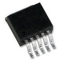
... National does not assume any responsibility for use of any circuitry described, no circuit patent licenses are implied and National reserves the right at any time without notice to change said circuitry and specifications. inches (millimeters) unless otherwise noted (Continued) Order Number LM2587S-3.3, LM2587S-5.0, LM2587S-12 or LM2587S-ADJ NS Package Number TS5B 2 ...