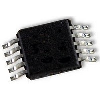
LM3481MM National Semiconductor, LM3481MM Datasheet - Page 18

LM3481MM
Manufacturer Part Number
LM3481MM
Description
IC, BOOST, CNTRL, 10MSOP
Manufacturer
National Semiconductor
Datasheet
1.LM3481EVALNOPB.pdf
(22 pages)
Specifications of LM3481MM
Primary Input Voltage
48V
No. Of Outputs
1
Output Current
1A
Voltage Regulator Case Style
MSOP
No. Of Pins
10
Operating Temperature Range
-40°C To +125°C
Svhc
No SVHC (15-Dec-2010)
Lead Free Status / RoHS Status
Lead free / RoHS Compliant
Available stocks
Company
Part Number
Manufacturer
Quantity
Price
Part Number:
LM3481MM
Manufacturer:
TI/德州仪器
Quantity:
20 000
Company:
Part Number:
LM3481MM/NOPB
Manufacturer:
TI
Quantity:
12 000
Part Number:
LM3481MMX
Manufacturer:
NS/国半
Quantity:
20 000
Company:
Part Number:
LM3481MMX/NOPB
Manufacturer:
TI
Quantity:
12 000
www.national.com
Designing SEPIC Using LM3481
Since the LM3481 controls a low-side N-Channel MOSFET,
it can also be used in SEPIC (Single Ended Primary Induc-
tance Converter) applications. An example of SEPIC using
the LM3481 is shown in
output voltage can be higher or lower than the input voltage.
The SEPIC uses two inductors to step-up or step-down the
input voltage. The inductors L1 and L2 can be two discrete
inductors or two windings of a coupled transformer since
equal voltages are applied across the inductor throughout the
switching cycle. Using two discrete inductors allows use of
catalog magnetics, as opposed to a custom transformer. The
input ripple can be reduced along with size by using the cou-
pled windings of transformer for L1 and L2.
Due to the presence of the inductor L1 at the input, the SEPIC
inherits all the benefits of a boost converter. One main ad-
vantage of SEPIC over a boost converter is the inherent input
to output isolation. The capacitor C
the output and provides protection against shorted or mal-
functioning load. Hence, the SEPIC is useful for replacing
boost circuits when true shutdown is required. This means
that the output voltage falls to 0V when the switch is turned
off. In a boost converter, the output can only fall to the input
voltage minus a diode drop.
The duty cycle of a SEPIC is given by:
In the above equation, V
FET, Q1, and V
POWER MOSFET SELECTION
As in a boost converter, the parameters governing the selec-
tion of the MOSFET are the minimum threshold voltage, V
DIODE
is the forward voltage drop of the diode.
Figure
Q
is the on-state voltage of the MOS-
17. As shown in
S
isolates the input from
FIGURE 17. Typical SEPIC Converter
Figure
17, the
TH
18
(MIN)
reverse transfer capacitance, C
to source voltage, V
SEPIC is given by:
The selected MOSFET should satisfy the condition:
The peak switch current is given by:
Where ΔI
rents of inductors L1 and L2 respectively.
The rms current through the switch is given by:
POWER DIODE SELECTION
The Power diode must be selected to handle the peak current
and the peak reverse voltage. In a SEPIC, the diode peak
current is the same as the switch peak current. The off-state
voltage or peak reverse voltage of the diode is V
Similar to the boost converter, the average diode current is
equal to the output current. Schottky diodes are recommend-
ed.
, the on-resistance, R
L1
and ΔI
V
SW(PEAK)
L2
V
are the peak-to-peak inductor ripple cur-
DS(MAX)
DS(MAX)
= V
DS(ON)
IN
. The peak switch voltage in a
> V
+ V
, the total gate charge, Q
RSS
SW(PEAK)
OUT
, and the maximum drain
+ V
DIODE
IN
+ V
g
, the
OUT
20136544
.


