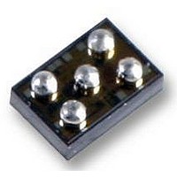
LM3677TL-ADJ National Semiconductor, LM3677TL-ADJ Datasheet - Page 19

LM3677TL-ADJ
Manufacturer Part Number
LM3677TL-ADJ
Description
IC, BUCK, REG, ADJ, 5USMD
Manufacturer
National Semiconductor
Datasheet
1.LM3677LEE-1.2NOPB.pdf
(24 pages)
Specifications of LM3677TL-ADJ
Primary Input Voltage
5.5V
No. Of Outputs
1
Output Voltage
3.3V
Output Current
600mA
Voltage Regulator Case Style
Micro SMD
No. Of Pins
5
Operating Temperature Range
-30°C To +85°C
Svhc
No SVHC
Lead Free Status / RoHS Status
Lead free / RoHS Compliant
Micro SMD Package Assembly And
Use
Use of the micro SMD package requires specialized board
layout, precision mounting and careful re-flow techniques, as
detailed in National Semiconductor Application Note 1112.
Refer to the section "Surface Mount Technology (SMD) As-
sembly Considerations". For best results in assembly, align-
ment ordinals on the PC board should be used to facilitate
placement of the device. The pad style used with micro SMD
package must be the NSMD (non-solder mask defined typ.).
This means that the solder-mask opening is larger than the
pad size. This prevents a lip that otherwise forms if the solder-
mask and pad overlap, from holding the device off the surface
of the board and interfering with mounting. See Application
Note 1112 for specific instructions how to do this. The 5-bump
package used for LM3677 has 300–micron solder balls and
requires 10.82 mils pads for mounting on the circuit board.
The trace to each pad should enter the pad with a 90° entry
angle to prevent debris from being caught in deep corners.
Initially, the trace to each pad should be 7 mil wide, for a sec-
tion approximately 7 mil long or longer, as a thermal relief.
Then each trace should neck up or down to its optimal width.
The important criteria is symmetry. This ensures the solder
bumps on the LM3677 re-flow evenly and that the device sol-
ders level to the board. In particular, special attention must be
Good layout for the LM3677 can be implemented by following
a few simple design rules, as illustrated in .
1.
Place the LM3677 on 10.82 mil pads. As a thermal relief,
connect to each pad with a 7 mil wide, approximately 7
mil long trace, and then incrementally increase each
trace to its optimal width. The important criterion is
FIGURE 9. Board Layout Design Rules for the LM3677
19
paid to the pads for bumps A1 and A3, because GND and
V
quate thermal relief can result in late or inadequate re-flow of
these bumps.
The micro SMD package is optimized for the smallest possi-
ble size in applications with red or infrared opaque cases.
Because the micro SMD package lacks the plastic encapsu-
lation characteristic of larger devices, it is vulnerable to light.
Backside metallization and/or epoxy coating, along with front-
side shading by the printed circuit board, reduce this sensi-
tivity. However, the package has exposed die edges. In
particular, micro SMD devices are sensitive to light, in the red
and infrared range, shining on the package’s exposed die
edges.
BOARD LAYOUT CONSIDERATIONS
PC board layout is an important part of DC-DC converter de-
sign. Poor board layout can disrupt the performance of a DC-
DC converter and surrounding circuitry by contributing to EMI,
ground bounce, and resistive voltage loss in the traces. These
can send erroneous signals to the DC-DC converter IC, re-
sulting in poor regulation or instability. Poor layout can also
result in re-flow problems leading to poor solder joints be-
tween the micro SMD package and board pads. Poor solder
joints can result in erratic or degraded performance.
2.
IN
are typically connected to large copper planes, inade-
symmetry to ensure the solder bumps on the re-flow
evenly (see Micro SMD Package Assembly and Use).
Place the LM3677, inductor and filter capacitors close
together and make the traces short. The traces between
these components carry relatively high switching
currents and act as antennas. Following this rule reduces
30008454
www.national.com


