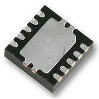
LT3481HDD Linear Technology, LT3481HDD Datasheet - Page 15

LT3481HDD
Manufacturer Part Number
LT3481HDD
Description
SW REG, 36V, 2A, 2.8MHZ, SD, 10DFN
Manufacturer
Linear Technology
Datasheet
1.LT3481HDD.pdf
(24 pages)
Specifications of LT3481HDD
Primary Input Voltage
34V
No. Of Outputs
1
Output Voltage
20V
Output Current
2A
Voltage Regulator Case Style
DFN
No. Of Pins
10
Operating Temperature Range
-40°C To +150°C
Svhc
No SVHC
Lead Free Status / RoHS Status
Lead free / RoHS Compliant
Available stocks
Company
Part Number
Manufacturer
Quantity
Price
Company:
Part Number:
LT3481HDD
Manufacturer:
LT
Quantity:
10 000
Part Number:
LT3481HDD#PBF
Manufacturer:
LINEAR/凌特
Quantity:
20 000
Part Number:
LT3481HDD#TRPBF
Manufacturer:
LINEAR/凌特
Quantity:
20 000
APPLICATIONS INFORMATION
may not be fully charged. Because the boost capacitor is
charged with the energy stored in the inductor, the circuit
will rely on some minimum load current to get the boost
circuit running properly. This minimum load will depend
on input and output voltages, and on the arrangement of
the boost circuit. The minimum load generally goes to
zero once the circuit has started. Figure 6 shows a plot
of minimum load to start and to run as a function of input
voltage. In many cases the discharged output capacitor
will present a load to the switcher, which will allow it to
start. The plots show the worst-case situation where V
is ramping very slowly. For lower start-up voltage, the
boost diode can be tied to V
input range to one-half of the absolute maximum rating
of the BOOST pin.
At light loads, the inductor current becomes discontinu-
ous and the effective duty cycle can be very high. This
reduces the minimum input voltage to approximately
300mV above V
current is continuous and the duty cycle is limited by the
maximum duty cycle of the LT3481, requiring a higher
input voltage to maintain regulation.
Figure 6. The Minimum Input Voltage Depends on
Output Voltage, Load Current and Boost Circuit
6.0
5.5
5.0
4.5
4.0
3.5
3.0
2.5
2.0
8.0
7.0
6.0
5.0
4.0
3.0
2.0
OUT
0.001
0.001
TO START
TO RUN
TO START
TO RUN
. At higher load currents, the inductor
0.01
0.01
LOAD CURRENT (A)
LOAD CURRENT (A)
IN
0.1
0.1
; however, this restricts the
V
T
L = 4.7μ
f = 800 kHz
V
T
L = 4.7μ
f = 800 kHz
OUT
A
OUT
A
1
1
= 25°C
= 25 °C
= 3.3V
= 5.0V
3481 F06
10
10
IN
Soft-Start
The RUN/SS pin can be used to soft-start the LT3481,
reducing the maximum input current during start-up.
The RUN/SS pin is driven through an external RC fi lter to
create a voltage ramp at this pin. Figure 7 shows the start-
up and shut-down waveforms with the soft-start circuit.
By choosing a large RC time constant, the peak start-up
current can be reduced to the current that is required to
regulate the output, with no overshoot. Choose the value
of the resistor so that it can supply 20μA when the RUN/SS
pin reaches 2.3V.
Synchronization
The internal oscillator of the LT3481 can be synchronized
to an external 275kHz to 475kHz clock by using a 5pF
to 20pF capacitor to connect the clock signal to the RT
pin. The resistor tying the RT pin to ground should be
chosen such that the LT3481 oscillates 20% lower than
the intended synchronization frequency (see Setting the
Switching Frequency section).
The LT3481 should not be synchronized until its output
is near regulation as indicated by the PG fl ag. This can be
done with the system microcontroller/microprocessor or
with a discrete circuit by using the PG output. If a sync
signal is applied while the PG is low, the LT3481 may
exhibit erratic operation. See Typical Applications
When applying a sync signal, positive clock transitions
reset LT3481’s internal clock and negative transitions
initiate a switch cycle. The amplitude of the sync signal
must be at least 2V. The sync signal duty cycle can range
0.22μF
RUN
Figure 7. To Soft-Start the LT3481, Add a Resisitor
and Capacitor to the RUN/SS Pin
15k
RUN/SS
GND
2ms/DIV
LT3481
3481 F07
I
1A/DIV
V
2V/DIV
V
2V/DIV
L
RUN/SS
OUT
15
3481fb


