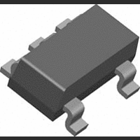
LM2611BMF National Semiconductor, LM2611BMF Datasheet - Page 7

LM2611BMF
Manufacturer Part Number
LM2611BMF
Description
IC, PWM INVERTING SWITCHING REG, SOT23-5
Manufacturer
National Semiconductor
Datasheet
1.LM2611AMFNOPB.pdf
(15 pages)
Specifications of LM2611BMF
Primary Input Voltage
5V
No. Of Outputs
1
Output Voltage
-36V
Output Current
1A
No. Of Pins
5
Operating Temperature Range
-40°C To +125°C
Supply Voltage Range
2.7V To 14V
Lead Free Status / RoHS Status
Contains lead / RoHS non-compliant
Available stocks
Company
Part Number
Manufacturer
Quantity
Price
Company:
Part Number:
LM2611BMF
Manufacturer:
NS
Quantity:
3 684
Company:
Part Number:
LM2611BMF
Manufacturer:
FAIRCHILD
Quantity:
1 469
Part Number:
LM2611BMF
Manufacturer:
NS/国半
Quantity:
20 000
Company:
Part Number:
LM2611BMFX
Manufacturer:
NS
Quantity:
5 321
Company:
Part Number:
LM2611BMFX
Manufacturer:
NS
Quantity:
21 534
Part Number:
LM2611BMFX
Manufacturer:
TI/德州仪器
Quantity:
20 000
Operation
The following equations define values given in Figure 2 and
Figure 3:
Use these equations to choose correct core sizes for the
inductors. The design of the LM2611’s internal compensa-
tion assumes L1 and L2 are equal to 10 - 22 µH, thus it is
recommended to stay within this range.
Switch Current Limit
The LM2611 incorporates a separate current limit compara-
tor, making current limit independent of any other variables.
The current limit comparator measures the switch current
versus a reference that represents current limit. If at any time
the switch current surpasses the current limit, the switch
opens until the next switching period. To determine the maxi-
mum load for a given set of conditions, both the input and
output inductor currents must be considered. The switch
current is equal to i
summary:
I
but will also be limited by the thermal resistivity of the
LM2611’s SOT23-5 package (θ
SW(PEAK)
Converter. The peak value is equal to the sum of the
average-to-peak current ripples through L1 and L2.
FIGURE 4. Switch Current Waveform in a Cuk
average currents through L1 and L2 and the
must be less than the current limit (1.2A typical),
(Continued)
L1
+ i
I
L2
L2
= I
, and is drawn in Figure 4. In
OUT
JA
= 265˚C/W).
20018102
7
Input Capacitor
The input current waveform to a Cuk converter is continuous
and triangular, as shown in Figure 2. The input inductor
insures that the input capacitor sees fairly low ripple cur-
rents. However, as the input inductor gets smaller, the input
ripple goes up. The RMS current in the input capacitor is
given by:
The input capacitor should be capable of handling the RMS
current. Although the input capacitor is not so critical in a Cuk
converter, a 10µF or higher value good quality capacitor
prevents any impedance interactions with the input supply. A
0.1µF or 1µF ceramic bypass capacitor is also recom-
mended on the V
be connected very close to pin 5 (within 0.2 inches).
Output Capacitor
Like the input current, the output current is also continuous,
triangular, and has low ripple (see I
capacitor must be rated to handle its RMS current:
For example, I
with 10µH ≤ L
V
analog supplies, see Split Supply Operation in the APPLI-
CATIONS section). The worst case conditions are with L
V
provide this level of RMS current, but ceramic capacitors are
ideally suited for the LM2611. Ceramic capacitors provide a
good combination of capacitance and equivalent series re-
sistance (ESR) to keep the zero formed by the capacitance
and ESR at high frequencies. The ESR zero is calculated as:
A general rule of thumb is to keep f
Cuk designs. Low ESR tantalum capacitors will usually be
rated for at least 180mA in a voltage rating of 10V or above.
However the ESR in a tantalum capacitor (even in a low ESR
tantalum capacitor) is much higher than in a ceramic capaci-
tor and could place f
run unstable.
Improving Transient Response/Compensation
The compensator in the LM2611 is internal. However, a
zero-pole pair can be added to the open loop frequency
response by inserting a feed forward capacitor, C
allel to the top feedback resistor (R
bandwidth can be improved with the added zero-pole pair.
This inturn will improve the transient response to a step load
change (see Figure 5 and Figure 6). The position of the
zero-pole pair is a function of the feedback resistors and the
capacitor value:
IN
OUT(MAX)
≤ 30V (V
, and V
IN
1,2
COUT(RMS)
may be 30V if using separate power and
≤ 22µH, −10V ≤ V
IN
IN(MAX)
pin (pin 5) of the IC. This capacitor must
ESR
low enough to cause the LM2611 to
. Many capacitor technologies will
can range from 30mA to 180mA
L2
ESR
OUT
FB1
in Figure 3). The output
). Phase margin and
>
≤ −3.3V, and 2.7V ≤
80kHz for LM2611
www.national.com
FF
, in par-
1,2
,


