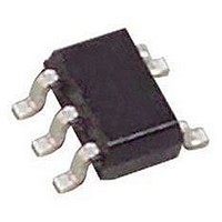
LM2733XMF National Semiconductor, LM2733XMF Datasheet - Page 10

LM2733XMF
Manufacturer Part Number
LM2733XMF
Description
IC, BOOST CONVERTER, 5-SOT-23
Manufacturer
National Semiconductor
Datasheet
1.LM2733XMFNOPB.pdf
(14 pages)
Specifications of LM2733XMF
Primary Input Voltage
5V
No. Of Outputs
1
Output Voltage
40V
Output Current
1A
No. Of Pins
5
Operating Temperature Range
-40°C To +125°C
Peak Reflow Compatible (260 C)
No
Lead Free Status / RoHS Status
Contains lead / RoHS non-compliant
Available stocks
Company
Part Number
Manufacturer
Quantity
Price
Company:
Part Number:
LM2733XMF
Manufacturer:
MINI
Quantity:
5 000
Part Number:
LM2733XMF
Manufacturer:
NS/国半
Quantity:
20 000
Company:
Part Number:
LM2733XMF/NOPB
Manufacturer:
NS
Quantity:
3 000
Part Number:
LM2733XMF/NOPB
Manufacturer:
TI/德州仪器
Quantity:
20 000
Company:
Part Number:
LM2733XMFX
Manufacturer:
NS
Quantity:
5 321
Company:
Part Number:
LM2733XMFX
Manufacturer:
NS
Quantity:
1 453
Part Number:
LM2733XMFX
Manufacturer:
NS/国半
Quantity:
20 000
Part Number:
LM2733XMFX/NOPB
Manufacturer:
TI/德州仪器
Quantity:
20 000
www.national.com
DUTY CYCLE
The maximum duty cycle of the switching regulator deter-
mines the maximum boost ratio of output-to-input voltage that
the converter can attain in continuous mode of operation. The
duty cycle for a given boost application is defined as:
This applies for continuous mode operation.
The equation shown for calculating duty cycle incorporates
terms for the FET switch voltage and diode forward voltage.
The actual duty cycle measured in operation will also be af-
fected slightly by other power losses in the circuit such as wire
losses in the inductor, switching losses, and capacitor ripple
current losses from self-heating. Therefore, the actual (effec-
tive) duty cycle measured may be slightly higher than calcu-
lated to compensate for these power losses. A good
approximation for effctive duty cycle is :
Where the efficiency can be approximated from the curves
provided.
INDUCTANCE VALUE
The first question we are usually asked is: “How small can I
make the inductor?” (because they are the largest sized com-
ponent and usually the most costly). The answer is not simple
and involves tradeoffs in performance. Larger inductors mean
less inductor ripple current, which typically means less output
voltage ripple (for a given size of output capacitor). Larger
inductors also mean more load power can be delivered be-
cause the energy stored during each switching cycle is:
Where “lp” is the peak inductor current. An important point to
observe is that the LM2733 will limit its switch current based
on peak current. This means that since lp(max) is fixed, in-
creasing L will increase the maximum amount of power avail-
able to the load. Conversely, using too little inductance may
limit the amount of load current which can be drawn from the
output.
Best performance is usually obtained when the converter is
operated in “continuous” mode at the load current range of
interest, typically giving better load regulation and less output
ripple. Continuous operation is defined as not allowing the in-
ductor current to drop to zero during the cycle. It should be
noted that all boost converters shift over to discontinuous op-
eration as the output load is reduced far enough, but a larger
inductor stays “continuous” over a wider load current range.
DC (eff) = (1 - Efficiency x (V
E =L/2 X (lp)
2
IN
/V
OUT
))
Basic Application Circuit
10
To better understand these tradeoffs, a typical application cir-
cuit (5V to 12V boost with a 10 µH inductor) will be analyzed.
We will assume:
V
Since the frequency is 1.6 MHz (nominal), the period is ap-
proximately 0.625 µs. The duty cycle will be 62.5%, which
means the ON time of the switch is 0.390 µs. It should be
noted that when the switch is ON, the voltage across the in-
ductor is approximately 4.5V.
Using the equation:
We can then calculate the di/dt rate of the inductor which is
found to be 0.45 A/µs during the ON time. Using these facts,
we can then show what the inductor current will look like dur-
ing operation:
During the 0.390 µs ON time, the inductor current ramps up
0.176A and ramps down an equal amount during the OFF
time. This is defined as the inductor “ripple current”. It can also
be seen that if the load current drops to about 33 mA, the
inductor current will begin touching the zero axis which means
it will be in discontinuous mode. A similar analysis can be
performed on any boost converter, to make sure the ripple
current is reasonable and continuous operation will be main-
tained at the typical load current values.
MAXIMUM SWITCH CURRENT
The maximum FET swtch current available before the current
limiter cuts in is dependent on duty cycle of the application.
This is illustrated in the graphs below which show both the
typical and guaranteed values of switch current for both the
"X" and "Y" versions as a function of effective (actual) duty
cycle:
IN
= 5V, V
OUT
= 12V, V
5V–12V Boost (LM2733X)
10 µH Inductor Current,
DIODE
V = L (di/dt)
20055405
= 0.5V, V
SW
= 0.5V
20055412


